Multi-level boost converter

Active Publication Date: 2019-07-11
HUAWEI DIGITAL POWER TECH CO LTD
View PDF18 Cites 17 Cited by
  • Summary
  • Abstract
  • Description
  • Claims
  • Application Information

AI Technical Summary

Benefits of technology

The patent text describes a new invention that improves upon existing technology. The invention solves certain problems or limitations that were present in the previous technology. The claimed subject matter is not limited to certain solutions and can be used in various applications.

Problems solved by technology

Although 1200V diodes that can handle the needed current and voltage levels are available, they are costly and have a number disadvantages.
In the case of a 1200V silicon diode, such devices show poor reverse recovery performance, allowing revers current flow and reducing efficiency.
In the case of a 1200V silicon carbide (SiC), the diode provides almost zero reverse recover, but has a high forward voltage drop.

Method used


Image

  • Multi-level boost converter
  • Multi-level boost converter
  • Multi-level boost converter

Examples


Embodiment Construction

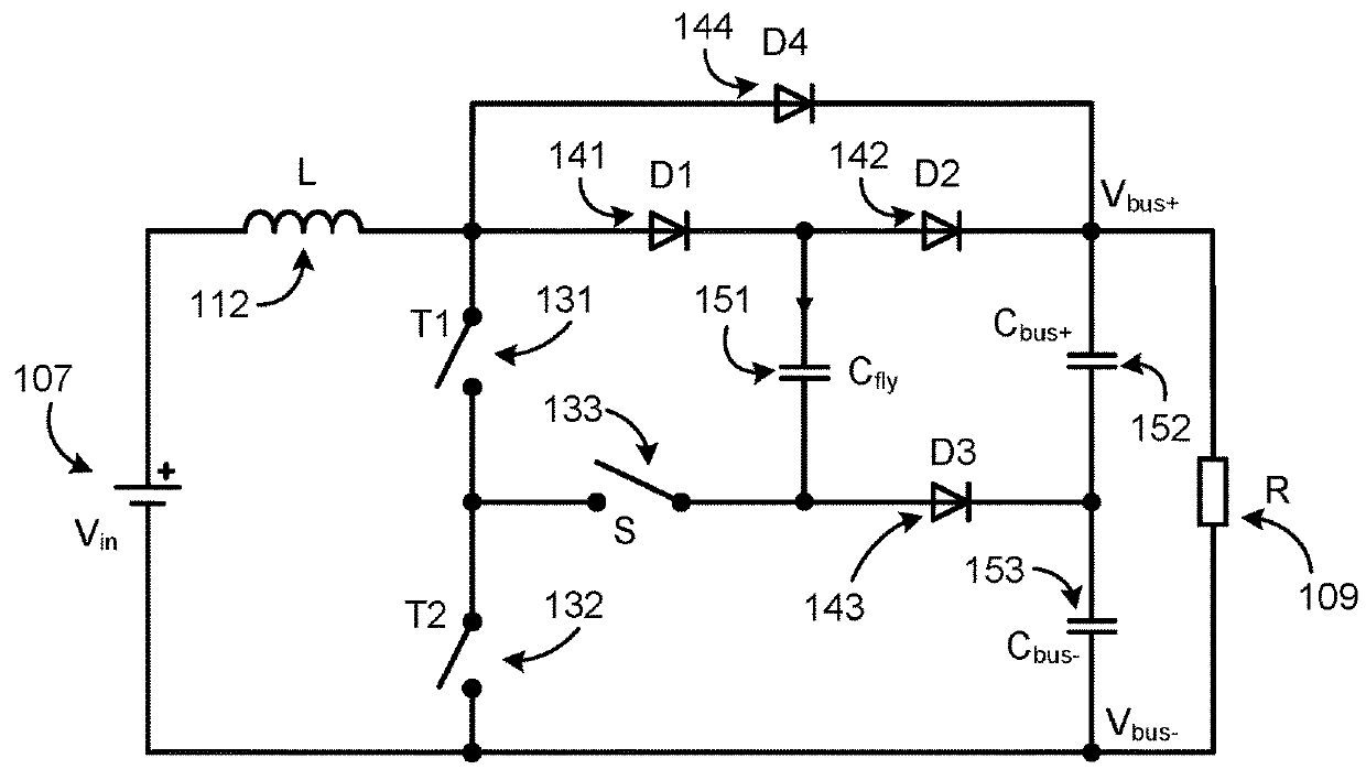
[0038]The following presents examples of boost converters with multi-level operation, placing components under lower stress voltages and allowing use of a smaller boost inductor. The boost inductor is connected to the output through a pair of series connected diodes, with a flying capacitor connected between the diodes on one side and to a multi-state waveform generated by a bridge circuit on an internal node on the other side. The internal node is connected to a capacitive voltage divider through a diode to protect the circuit from voltage surges on the output node. The boost convert includes a pre-charge path for the flying capacitor. In parallel with the series connected diodes, another diode is connected in parallel to reduce conduction loses.

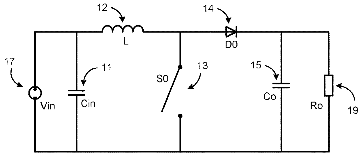
[0039]The embodiments of multi-level boost converters presented can be used across a wide range of voltage levels, including for high voltage levels. For example, they can be applied to power supply systems requiring a regulated output volt...


PUM


Abstract

A DC to DC converter uses a multi-level boost converter topology. In addition to the input voltage being connected to an output node through a boost inductor in series with a pair of diodes, a bridge circuit generates a multi-level waveform on one side of flying capacitor, which is on the other side connected between the series connected diodes. The boost converter topology maintains low voltage stress on its components under abnormal conditions on the output node and allows for simple pre-charging of the flying capacitor.

Description

BACKGROUND[0001]The following is related generally to the field of DC to DC converters and, more specifically, to boost converters.PRIOR ART[0002]Boost converters are a type of DC to DC electric power converter that generate an output voltage higher than the input voltage, at the cost of a lower current level. FIG. 1 shows an example of a boost converter.[0003]In this example, the input voltage source Vin 17 is connected to the ground or low voltage rail at the − terminal and connected to the load at the + terminal, represented by the resistor Ro 19, through the series combination of an inductor L 12 and a diode D014. An output capacitor Co 15 is connected between the output node at Vo and ground, in parallel with the load Ro 19, and an input capacitor Cin 11 is connected between the input and ground, in parallel with the voltage source Vin 17. A switch S013 is connected on the one side to a node between the inductor L 12 and the diode D014, and on the other side to ground. The swit...

Claims


Application Information

Patent Timeline
IPC IPC(8): H02M3/158H02M1/08
CPCH02M1/32H02M2001/0048H02M3/158H02M1/36H02M3/07H02M1/0048H02M1/0095H02M7/4837Y02B70/10
Inventor YU, BOZHAN, JINXIANGFU, DIANBO
Owner HUAWEI DIGITAL POWER TECH CO LTD
Why Eureka
Try Eureka