Single photon avalanche diode control circuit
- Summary
- Abstract
- Description
- Claims
- Application Information
AI Technical Summary
Benefits of technology
Problems solved by technology
Method used
Image
Examples
embodiment 1
[0029]An embodiment of the present disclosure will be described in detail below.
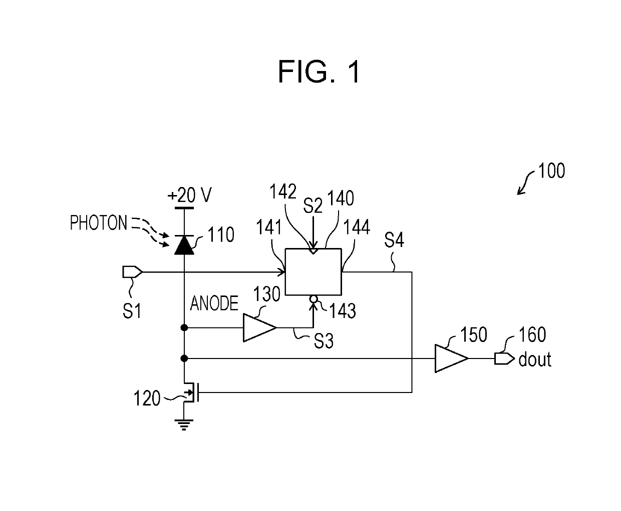
[0030]FIG. 1 illustrates an exemplary circuit configuration of a SPAD control circuit 100 according to Embodiment 1. FIG. 1 illustrates an exemplary configuration of the SPAD control circuit 100 in which a bias voltage of about +20 V is applied to the cathode of a SPAD 110, and photon detections are read out from the anode of the SPAD 110.
Configuration of SPAD Control Circuit 100
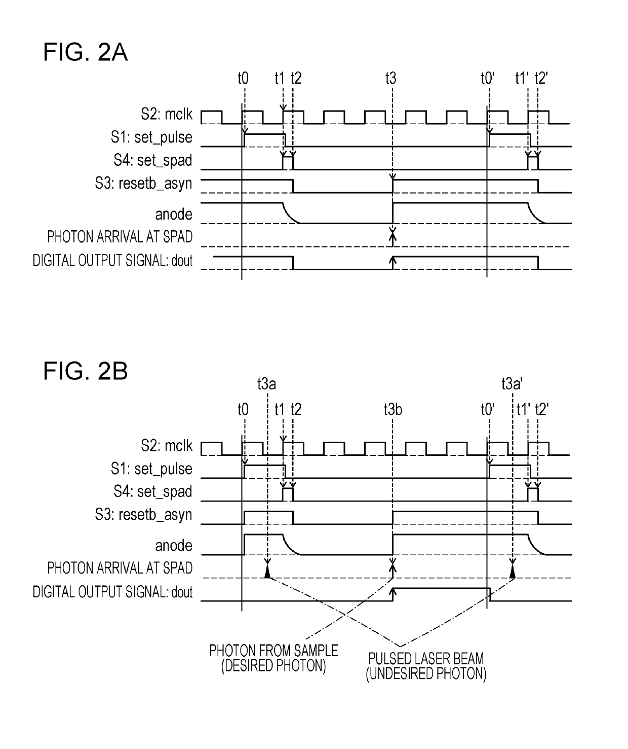
[0031]As illustrated in FIG. 1, the SPAD control circuit 100 includes a combinational circuit (a buffer 150) for reading a change in anode voltage due to avalanche breakdown, and outputting the change in voltage to an output terminal 160 as a digital output signal dout, a combinational circuit (a buffer 130) for reading a change in anode voltage, and outputting the change in voltage to a sequential circuit described later, a switch (a transistor 120) for biasing the anode of the SPAD 110 to 0 V in accordance with the state of the...
embodiment 2
[0040]Another embodiment of the present disclosure will be described below. For the convenience of explanation, components that are identical in function to the components described above with reference to Embodiment 1 will be designated by the same reference signs, and a description of such components will not be repeated.
Configuration of SPAD Control Circuit 300
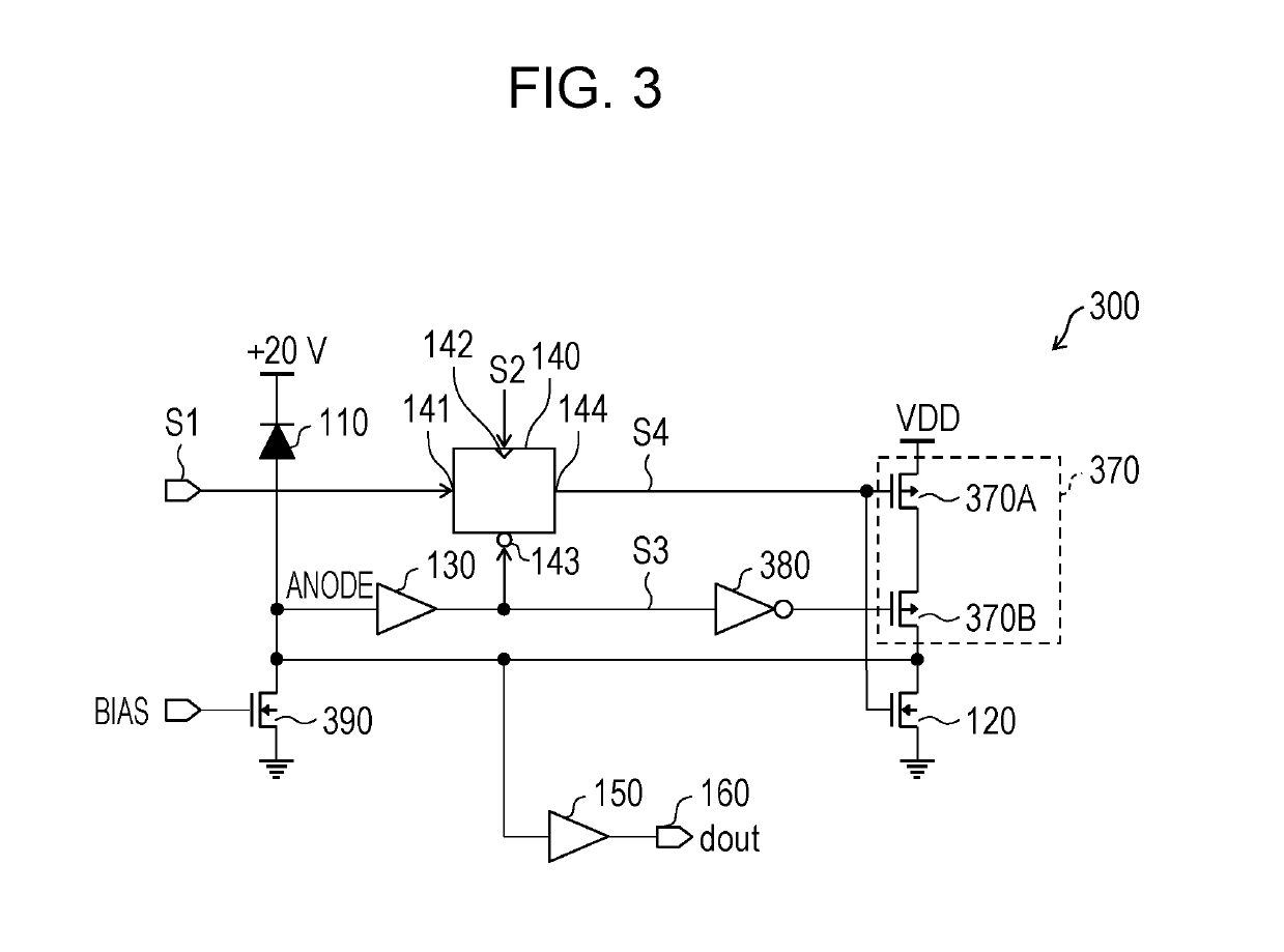
[0041]FIG. 3 illustrates a SPAD control circuit 300. The SPAD control circuit 300 includes the following components further added to the SPAD control circuit 100 illustrated in FIG. 1: an nch transistor 390 (which functions as a high resistance) that biases the anode of the SPAD 110 to 0 V; a switch 370 (pch transistors 370A and 370B) for biasing the anode of the SPAD 110 to the voltage VDD in accordance with the state of the SPAD 110; and a combinational circuit (inverter 380).
[0042]The output signal S3 (resetb_asyn) from the buffer 130 is input to the inverter 380. An output signal from the inverter 380 is input to the ga...
embodiment 3
[0045]A still another embodiment of the present disclosure will be described below. For the convenience of explanation, components that are identical in function to the components described above with reference to Embodiments 1 and 2 will be designated by the same reference signs, and a description of such components will not be repeated.
Configuration of SPAD Control Circuit 400
[0046]FIG. 4 illustrates a configuration of a SPAD control circuit 400 according to Embodiment 3. In the configuration illustrated in FIG. 4, the inverter 380, which is one embodiment of a combinational circuit in the SPAD control circuit illustrated in FIG. 3, is replaced with a NOR gate 480, and the buffer 150, which is one embodiment of a combinational circuit connected to the digital output signal dout, is replaced with a combinational circuit 450 including a NOR gate 450A and an AND gate 450B.
[0047]The output signal S3 (resetb_asyn) from the buffer 130 is input to a first input terminal of the NOR gate 4...
PUM
 Abstract
Description
Claims
Application Information


