Annular-gate single-photon avalanche diode capable of preventing edge breakdown and preparation method of annular-gate single-photon avalanche diode capable of preventing edge breakdown

A single-photon avalanche, photodiode technology, applied in semiconductor/solid-state device manufacturing, electrical components, circuits, etc., can solve problems such as guard ring depletion, incompatibility, device performance degradation, etc., to improve detection efficiency and device performance. , the effect of reducing lattice defects

Inactive Publication Date: 2017-02-22
TIANJIN UNIV
View PDF1 Cites 29 Cited by
  • Summary
  • Abstract
  • Description
  • Claims
  • Application Information

AI Technical Summary

Problems solved by technology

The former is not compatible with the standard CMOS process, and the currently used guard ring structure is mainly realized by introducing an additional low-doped well region or shallow trench isolation (STI) at the edge of the photosensitive region.
Guard rings implemented using low doped well region

Method used


Image

  • Annular-gate single-photon avalanche diode capable of preventing edge breakdown and preparation method of annular-gate single-photon avalanche diode capable of preventing edge breakdown
  • Annular-gate single-photon avalanche diode capable of preventing edge breakdown and preparation method of annular-gate single-photon avalanche diode capable of preventing edge breakdown
  • Annular-gate single-photon avalanche diode capable of preventing edge breakdown and preparation method of annular-gate single-photon avalanche diode capable of preventing edge breakdown

Examples


Embodiment 1

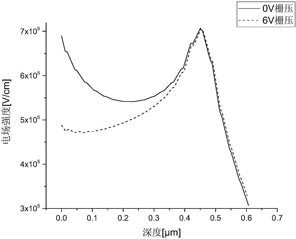
[0039] Embodiments of the present invention provide a single photon avalanche diode detector structure that can effectively suppress edge breakdown and is compatible with a standard CMOS process. The detector consists of a N-well in a deep N-well + / P-well structure built photodiode and ring gate electrode. When the device is working, the voltage on the ring gate is added to reduce the electric field at the edge of the photosensitive area, thereby suppressing edge breakdown. In addition, the device structure proposed by the embodiments of the present invention can also flexibly adjust the gate voltage, so that the SPAD can adapt to different overbias voltages.

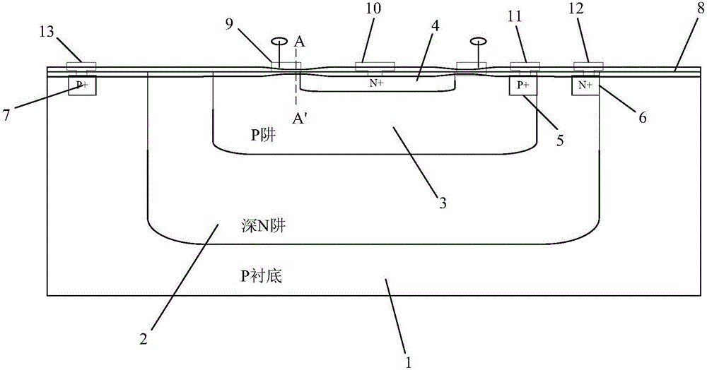
[0040] The structure of the single photon avalanche diode detector described in the embodiment of the present invention is as follows: figure 1 shown. detector by N + / P-well constitutes the photosensitive area, and by controlling the N + / P-well type photodiode around the ring gate voltage to weaken the fringe el...

Embodiment 2

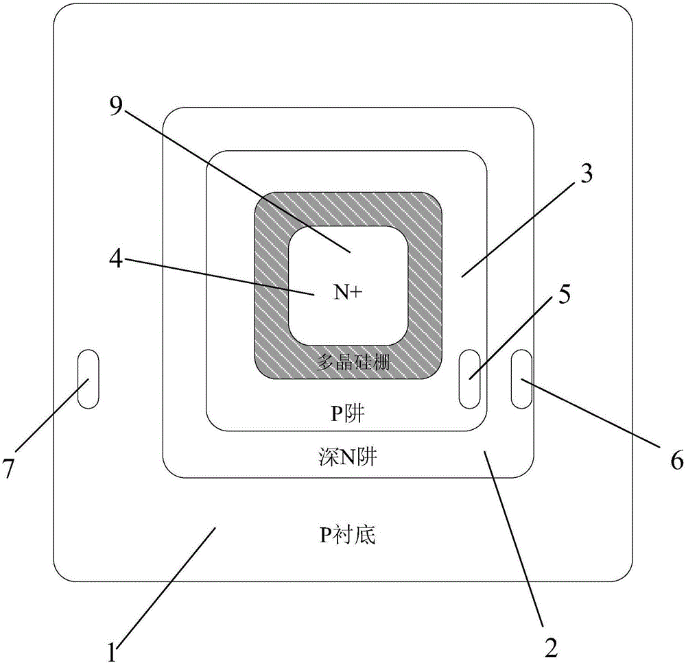
[0044] For ease of description, the embodiments of the present invention will be further described in detail below in conjunction with the accompanying drawings. figure 1 and figure 2 are the cross-section and top view of the detector respectively, for the convenience of explanation, figure 2 The oxide layer 8 and the metal electrodes 10, 11, 12 and 13 are not shown.

[0045]In the illustration, 1 is the substrate. The substrate material is a P-type lightly doped silicon wafer, which is used as the supporting part of the designed single photon avalanche diode. In the illustration, 2 is a deep N well. On the one hand, the deep N well is used as a local substrate of the photodiode, and on the other hand, it is also used to realize the mutual isolation of the detector and other electronic devices. In the illustration, 3 is the P well region, and the P well adopts a medium doping concentration. In the illustration, 4 is a heavily doped N region, which together with the above...

Embodiment 3

[0067] The embodiment of the present invention also provides a method for manufacturing the photodetector, the main process steps of which include:

[0068] 1) A lightly doped deep N well 2 is formed on a P-type lightly doped silicon substrate 1 by using standard CMOS processes such as oxidation, photolithography, ion implantation, and annealing, so as to realize electrical isolation from other electronic devices and avoid their mutual influences;

[0069] 2) Prepare a moderately doped P-type well region 3 in the above-mentioned deep N well region, and then regenerate a silicon dioxide thin layer;

[0070] 3) Fabricate the annular polysilicon gate 9 . First, a layer of polysilicon is deposited on the newly grown gate oxide layer by chemical vapor deposition (CVD), and then the pattern of the polysilicon gate 9 is prepared by dry etching technology;

[0071] 4) Prepare N-type heavily doped contact region 4 in P-type well region 3 to form N + / P-well type photodiode, the N-ty...


PUM


Abstract

The invention discloses an annular-gate single-photon avalanche diode capable of preventing edge breakdown and a preparation method of the annular-gate single-photon avalanche diode capable of preventing edge breakdown. A heavily-doped N-region and a P-well region jointly form an N<+>/P-well type photodiode structure; the heavily-doped N-region also serves as a cathode contact region of an photoelectric detector; a P-well contact region is a heavily-doped P-type region and serves as an anode contact region of the photoelectric detector; in an electric field of an avalanche region, the heavily-doped N<+> region points to the P-well region, so that electrons generated below a depletion region drift into the avalanche regions more easily, and sensitivity of the detector is improved; a deep N-well serves as a local substrate of the photodiode and is used for isolating the photodiode from other electron devices; an oxidation layer region comprises a gate oxide portion and a field oxide portion; a polysilicon gate is an annular region enclosing the photodiode; a depletion layer of an N<+>/P-well type photodiode serves as a main photosensitive region during single-photon detection. The annular-gate single-photon avalanche diode is capable of preventing edge breakdown from affecting normal operation of an SPAD (single-photon avalanche diode).

Description

technical field [0001] The invention relates to the fields of photoelectric detection and image sensors, in particular to a single-photon avalanche diode (SPAD) structure compatible with a standard complementary metal-oxide-semiconductor (CMOS) process, and the use of oxidation, photolithography in the standard CMOS process , etching, ion implantation, metallization and other processes to achieve the preparation method. Background technique [0002] Single photon detection is to amplify a single photon signal and identify it through pulse discrimination and digital counting techniques, so as to achieve the ultimate sensitivity of photoelectric detection. Single photon detection has become one of the most active research fields in the international community due to its great scientific value and strategic position. application. Designing efficient and reliable single-photon detectors is one of the key issues in single-photon detection technology. [0003] Due to the extrem...

Claims


Application Information

Patent Timeline
IPC IPC(8): H01L29/861H01L21/329H01L29/06H01L31/107
Inventor 谢生吴佳骏毛陆虹
Owner TIANJIN UNIV
Why Eureka
Try Eureka