

Single photon avalanche diode with second semiconductor layer burried in epitaxial layer
a single-photon avalanche and epitaxial layer technology, applied in semiconductor devices, radio frequency control devices, electrical apparatuses, etc., can solve the problems of low time resolution, difficulty in forming high electric field areas, and small aperture ratio of spad arrays compared to two-dimensional array structures, etc., to achieve the effect of reducing distance between neighboring spad arrays, reducing the width of depletion layers, and increasing aperture ratios
- Summary
- Abstract
- Description
- Claims
- Application Information
AI Technical Summary
Benefits of technology
Problems solved by technology
Method used
Image

Examples
first embodiment
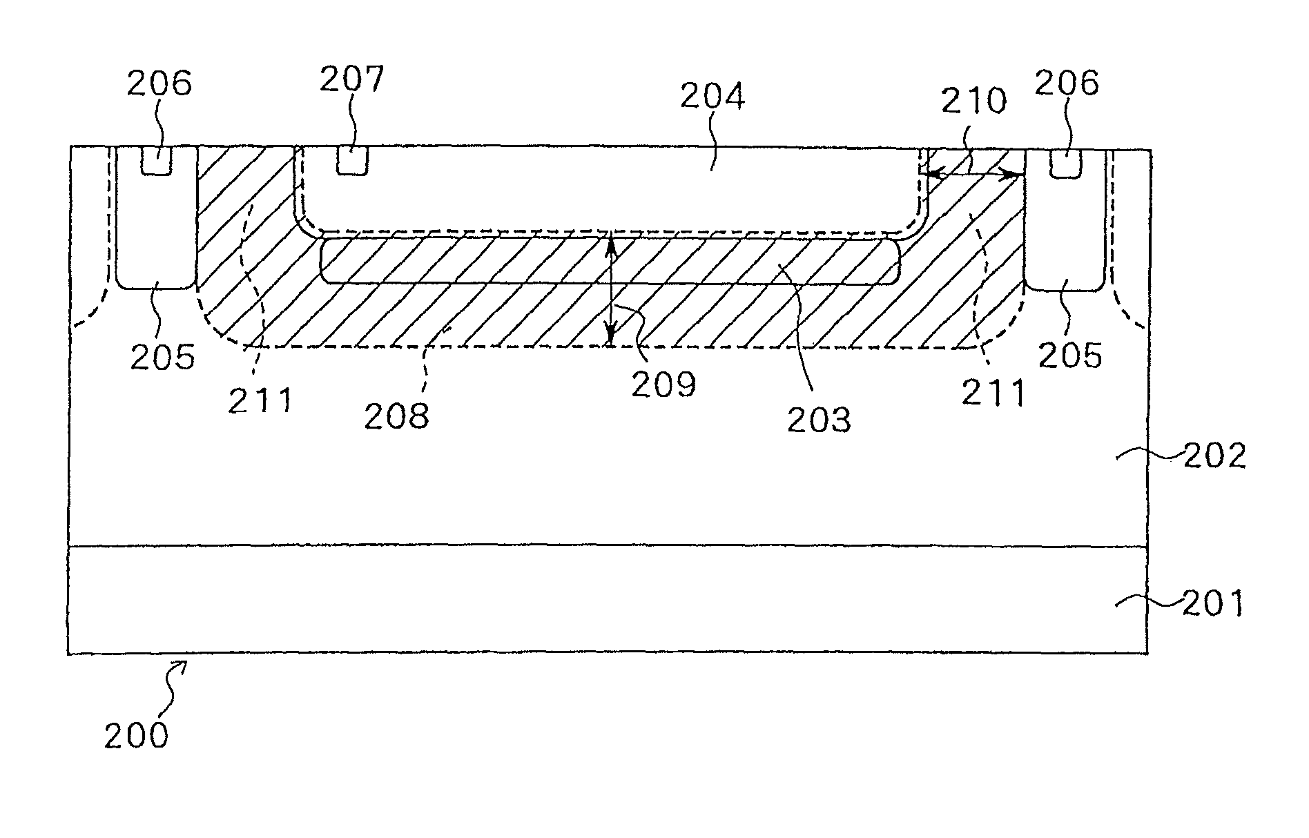
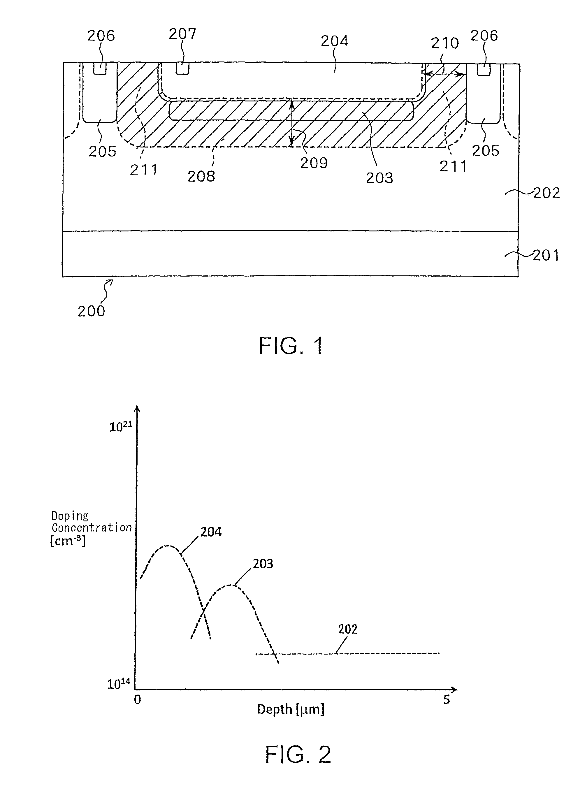
[0032]FIG. 1 is a cross-sectional view illustrating a SPAD according to a first embodiment of the present invention. The SPAD according to the present embodiment includes a second semiconductor layer 203 that is buried within an epitaxial layer 202 and of the same conductivity type as the epitaxial layer 202. Further, the SPAD illustrated in FIG. 1 includes a first semiconductor layer 204 that is implanted above the second semiconductor layer 203 and is of the opposite conductivity type to the epitaxial layer 202. The epitaxial layer 202 is a layer that has grown on a silicon substrate 201. The silicon substrate 201 is of the same type as the epitaxial layer 202. It is preferred that the second semiconductor layer 203, the epitaxial layer 202, and the silicon substrate 201 be of p-type conductivity. On the other hand, it is preferred that the first semiconductor layer 204 be of n-type conductivity. The SPAD formed by the first semiconductor layer 204 and the second semiconductor lay...
second embodiment
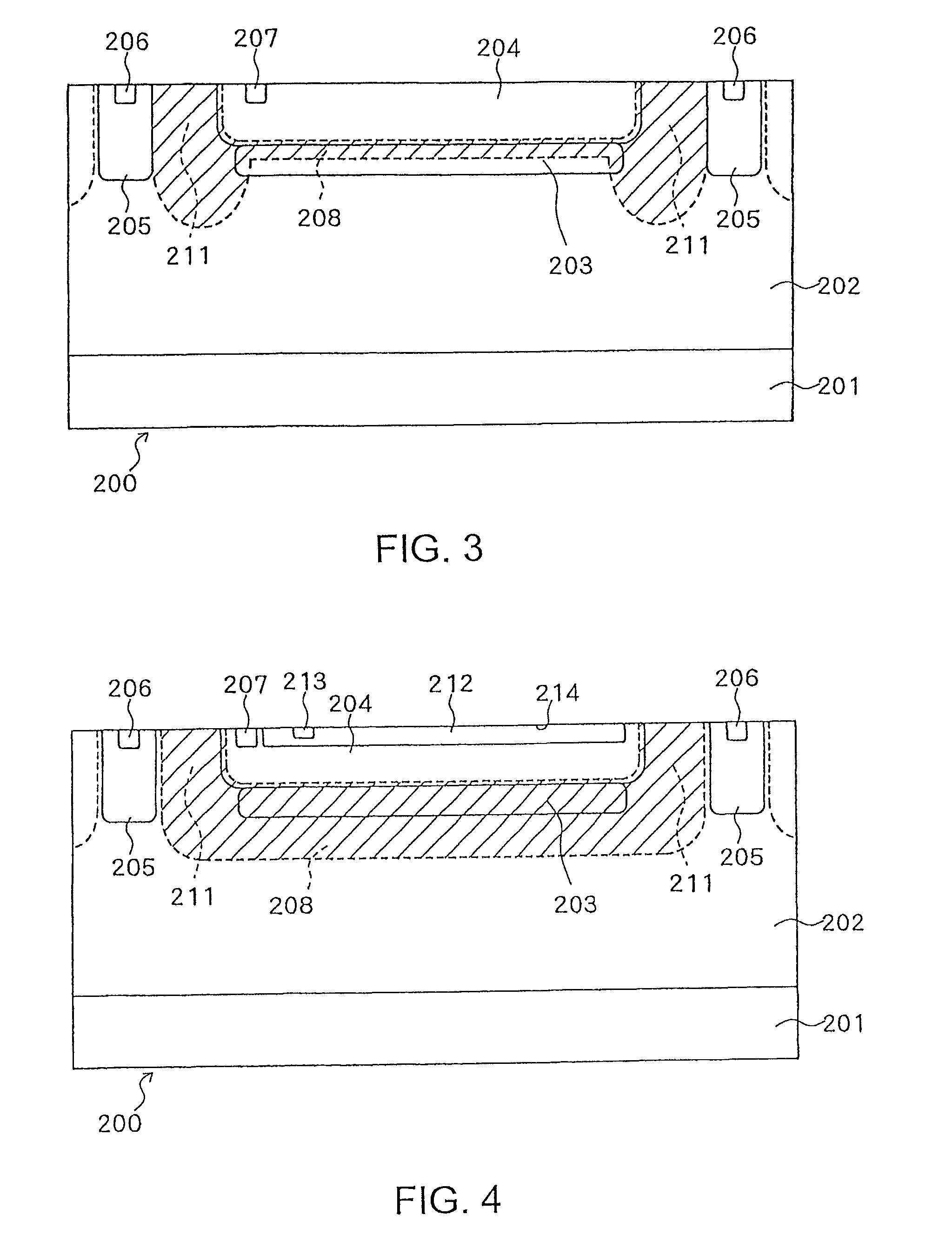
[0042]FIG. 4 illustrates a SPAD configuration according to a second embodiment of the present invention. According to the SPAD configuration illustrated in FIG. 4, all of the second semiconductor layer 203, the third semiconductor layer 205, the epitaxial layer 202, and the substrate 201 are of p-type conductivity and the first semiconductor layer 204 is of n-type conductivity. In the present embodiment, a fourth semiconductor layer 212 is formed within the first semiconductor layer 204 of the SPAD. The fourth semiconductor layer 212 is shallow in shape and is of p-type conductivity. The fourth semiconductor layer 212 is formed in such a way as to sufficiently overlap the avalanche multiplication area formed between the first semiconductor layer 204 and the second semiconductor layer 203. At least one electrode 213 may be provided to connect the fourth semiconductor layer 212.
[0043]FIG. 5 illustrates an example of the doping profile of the SPAD according to the present embodiment. A...
third embodiment
[0047]FIG. 6 illustrates a SPAD configuration according to a third embodiment of the present invention. The SPAD illustrated in FIG. 6 is characteristically similar to the SPADs described in the above-mentioned embodiments.
[0048]In the present embodiment, the isolation of neighboring SPADs is implemented by a combination of the third semiconductor layer 205 and a buried isolation layer 215, instead of using only the third semiconductor layer 205. The third semiconductor layer 205 and the buried isolation layer 215 are of the same conductivity type and are stacked in the vertical direction. It is desired that the third semiconductor layer 205 and the buried isolation layer 215 are of p-type conductivity. The vertically stacked layers 205 and 215 can effectively prevent the depletion layer 208 of one SPAD from contacting the depletion layer 208 of a neighboring SPAD. In other words, the SPAD illustrated in FIG. 6 can improve the isolation between neighboring SPADs.
PUM
 Abstract
Description
Claims
Application Information