
Method for depositing a material film on a substrate within a reaction chamber by a cyclical deposition process and related device structures

a technology of cyclical deposition and reaction chamber, which is applied in the direction of chemical vapor deposition coating, coating, transistor, etc., can solve the problems of nmos and pmos devices not showing ideal effective work functions, polysilicon may not be ideal gate electrode material for advanced technology node applications, and the threshold voltage adjustment implantation process may become increasingly complex

Active Publication Date: 2019-07-18
ASM IP HLDG BV
View PDF3 Cites 242 Cited by
  • Summary
  • Abstract
  • Description
  • Claims
  • Application Information

AI Technical Summary

Benefits of technology

The patent is about a method for depositing a material film onto a substrate using a cyclical deposition process. The method involves contacting the substrate with a first vapor phase reactant and then purging the reaction chamber with a first main purge. Next, the substrate is contacted with a second vapor phase reactant using micro pulsing, where each micro pulse provides a substantially constant concentration of the second reactant to the reaction chamber. This process is repeated, followed by another main purge and then a second micro purge to achieve a final material film with desired properties. The method may provide advantages such as improved deposition control and stability, as well as reduced damage to the substrate.

Problems solved by technology

However, doped polysilicon may not be an ideal gate electrode material for advanced technology node applications.
As a further example, polysilicon does not exhibit an ideal effective work function (eWF) for both NMOS and PMOS devices.
However, as device geometries reduce in advanced technology node applications, the threshold voltage adjustment implantation processes may become increasingly complex.
However, it is not straightforward to uniformly deposit materials directly over high aspect ratio device structures in order to create material films that meet certain specifications for a desired application.
For example, when utilizing an atomic layer deposition process to deposit a conformal material film over a device structure including high aspect ratio features it may be challenging to supply a vapor phase reactant consistently, pulse after pulse, with enough vapor concentration to ensure conformal, uniform, deposition over the high aspect ratio features, especially in the bottom of deep trench features.

Method used


Image

  • Method for depositing a material film on a substrate within a reaction chamber by a cyclical deposition process and related device structures
  • Method for depositing a material film on a substrate within a reaction chamber by a cyclical deposition process and related device structures
  • Method for depositing a material film on a substrate within a reaction chamber by a cyclical deposition process and related device structures

Examples


Embodiment Construction

[0016]Although certain embodiments and examples are disclosed below, it will be understood by those in the art that the invention extends beyond the specifically disclosed embodiments and / or uses of the invention and obvious modifications and equivalents thereof. Thus, it is intended that the scope of the invention disclosed should not be limited by the particular disclosed embodiments described below.

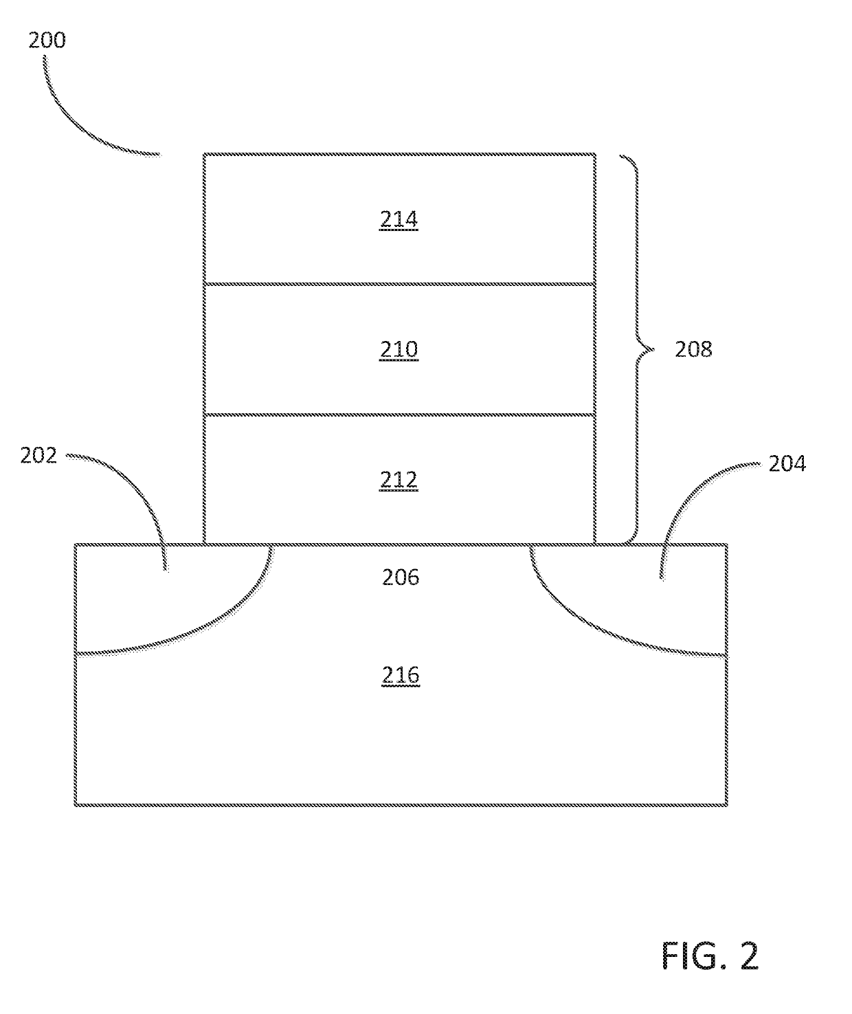
[0017]The illustrations presented herein are not meant to be actual views of any particular material, structure, or device, but are merely idealized representations that are used to describe embodiments of the disclosure.

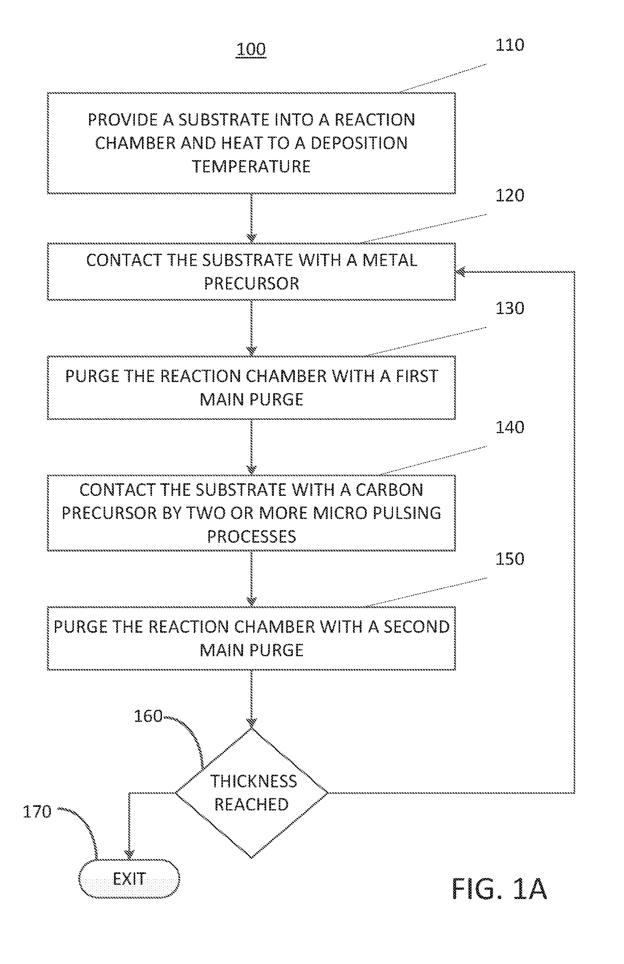
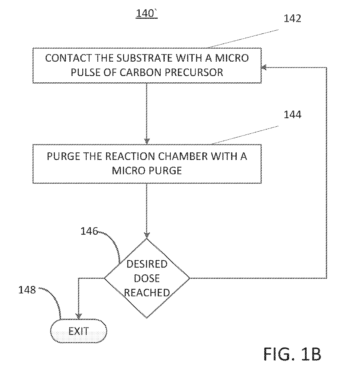
[0018]As used herein, the term “cyclic deposition” may refer to the sequential introduction of precursors (reactants) into a reaction chamber to deposit a film over a substrate and includes deposition techniques such as atomic layer deposition and cyclical chemical vapor deposition.

[0019]As used herein, the term “cyclical chemical vapor deposition” may refer to any pro...


PUM

PropertyMeasurementUnit
Fractionaaaaaaaaaa
Timeaaaaaaaaaa
Timeaaaaaaaaaa

Abstract

A method of depositing a material film on a substrate within a reaction chamber by a cyclical deposition process is disclosed. The method may include: contacting the substrate with a first vapor phase reactant and purging the reaction chamber with a first main purge. The method also includes: contacting the substrate with a second vapor phase reactant by two or more micro pulsing processes, wherein each micro pulsing process comprises: contacting the substrate with a micro pulse of a second vapor phase reactant; and purging the reaction chamber with a micro purge, wherein each of the micro pulses of the second vapor phase reactant provides a substantially constant concentration of the second vapor phase reactant into the reaction chamber. The method may also include; purging the reaction chamber with a second main purge. Device structures including a material film deposited by the methods of the disclosure are also disclosed.

Description

CROSS-REFERENCE TO RELATED APPLICATION[0001]This application claims the benefit of U.S. Provisional Application No. 62 / 617,959, entitled “METHOD FOR DEPOSITING A MATERIAL FILM ON A SUBSTRATE WITHIN A REACTION CHAMBER BY A CYCLICAL DEPOSITION PROCESS AND RELATED DEVICE STRUCTURES” and filed on Jan. 16, 2018, the disclosure of which is hereby incorporated herein for reference.FIELD OF INVENTION[0002]The present disclosure relates generally to methods for depositing a material film on a substrate within a reaction chamber by a cyclical deposition process and particularly methods for depositing transition metal aluminum carbide films by a cyclical deposition process. The present disclosure is also related generally to device structures comprising a material film deposited by a cyclical deposition process.BACKGROUND OF THE DISCLOSURE[0003]Complementary metal-oxide-semiconductor (CMOS) technology has conventionally utilized n-type and p-type polysilicon as the gate electrode material. How...

Claims


Application Information

Patent Timeline
IPC IPC(8): H01L21/285H01L29/49H01L21/28C23C16/32C23C16/455
CPCH01L21/28556H01L29/4966H01L21/28088C23C16/32C23C16/45553C23C16/45527H01L29/78C23C16/45525H01L21/0228H01L21/02205H01L21/8238H01L27/092H01L2924/01022H01L2924/01013H01L2924/01006
Inventor RAISANEN, PETRIOLSTAD, MARKROMERO, JOSE ALEXANDROLI, DONGJOHNSON, WARDCHEN, PEIJUN
Owner ASM IP HLDG BV
Features
  • Generate Ideas
  • Intellectual Property
  • Life Sciences
  • Materials
  • Tech Scout
  • Unparalleled Data Quality
  • Higher Quality Content
  • 60% Fewer Hallucinations
Learn More