Image pickup device and display device

a technology of image pickup and display device, which is applied in the direction of image enhancement, radiation control device, instruments, etc., can solve the problems of insufficient moisture resistance performance of these materials, inability to completely block the entrance of moisture from the side wall portion, and silicon nitride film may deteriorate the optical characteristics of the solid-state image pickup device. , to achieve the effect of improving the moisture resistan

Inactive Publication Date: 2019-07-25
CANON KK
View PDF7 Cites 0 Cited by
  • Summary
  • Abstract
  • Description
  • Claims
  • Application Information

AI Technical Summary

Benefits of technology

[0027]According to the present invention, it is possible to provide an image pickup devic

Problems solved by technology

However, when a silicon oxide film, for example, is used as a protective film that covers a side wall portion vertical to the surface of a substrate, it is not possible to completely block entrance of moisture from the side wall portion.
In particular, when a material component (for example, a dye-based material) sensitive to moisture is used as a color filter layer used in a solid state image pickup device, the moisture resistance performance of these materials is sometimes insufficient.
However, although a silicon nitride film is more effective tha

Method used


Image

  • Image pickup device and display device
  • Image pickup device and display device
  • Image pickup device and display device

Examples


embodiment 1

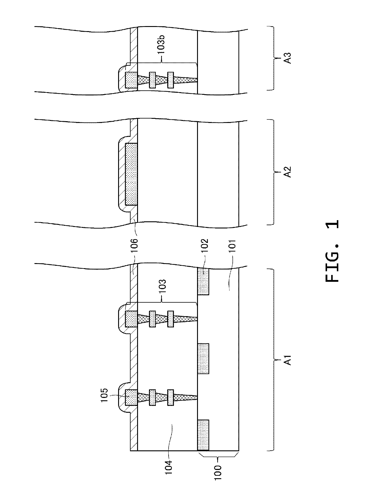
[0051]FIGS. 1 to 6 illustrate cross-sectional schematic diagrams of a front-illuminated solid state image pickup device according to the present embodiment in process order. In FIG. 1, a semiconductor substrate 100 includes a first semiconductor region 101 and a second semiconductor region 102. The first semiconductor region 101 is a region shared by a plurality of photoelectric converting portions. The second semiconductor region 102 is configured as a semiconductor region of the opposite conductivity type from the first semiconductor region and forms a PN junction with the first semiconductor region 101. The second semiconductor region 102 is a region in which carriers of the same polarity as signal charges are majority carriers.

[0052]Although not illustrated in the drawing, an element separating region is disposed between adjacent second semiconductor regions 102 to electrically separate the second semiconductor regions 102. Insulation film separation such as LOCOS separation or ...

embodiment 2

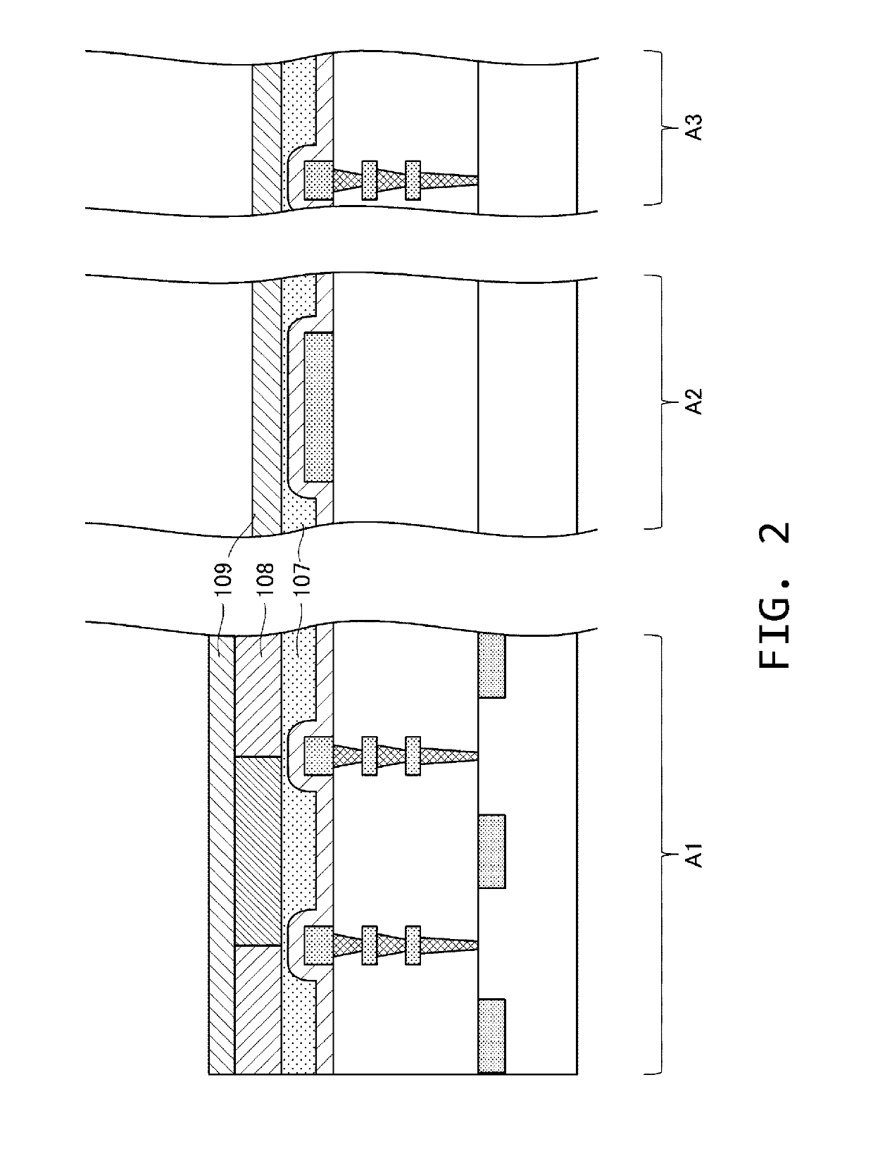
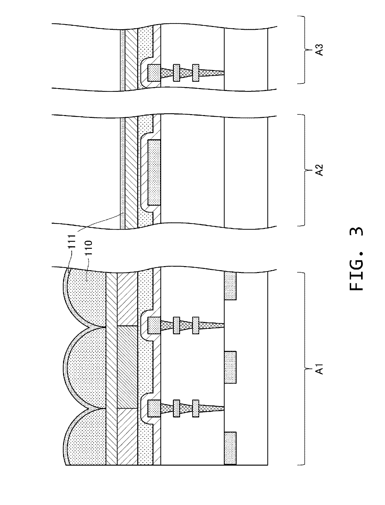
[0076]Hereinafter, Embodiment 2 will be described focusing on the difference from Embodiment 1. FIGS. 7 to 11 illustrate a manufacturing method of a solid state image pickup device according to the present embodiment. As illustrated in FIG. 11, a solid state image pickup device of the present embodiment is different from that of Embodiment 1 in that the uppermost-surface metal film 212 continuously covers the pad electrode region A2 and the scribing region and effective chip boundary portion A3. Moreover, an inorganic film 208 side wall portion is disposed between the uppermost-surface metal film 212 and the side wall portion or the ceiling portion. In this way, a two-layer structure of an inorganic insulating film and a metal film is formed.

[0077]The description will be continued with reference to FIG. 7. The manufacturing method of Embodiment 2 up to the process of forming the on-chip microlens 110 is the same as that of Embodiment 1.

[0078]Subsequently, in Embodiment 1, the inorga...

embodiment 3

[0088]In the present embodiment, a so-called back-illuminated solid state image pickup device is presented as a solid state image pickup device. The solid state image pickup device illustrated in FIG. 14 includes a first semiconductor substrate B1 in which a first transistor and a photoelectric converting element are disposed and a second semiconductor substrate B2 in which a second transistor is disposed. A surface on which the first transistor of the first semiconductor substrate B1 is disposed and a surface on which the second transistor of the second semiconductor substrate B2 is disposed are disposed to face each other. The solid state image pickup device of FIG. 14 is divided into a pixel region C1, a driving circuit region C2, and an electrode pad region C3.

[0089]A first planarizing layer 301 formed of an organic material, a color filter layer 302, a second planarizing layer 303, and an on-chip microlens layer 304 are stacked on the semiconductor substrate. The color filter l...


PUM


Abstract

Provided is an image pickup device including: a semiconductor substrate including a pixel region in which pixels are arranged and a pad electrode region on which a pad electrode portion is disposed; a wiring layer formed on the semiconductor substrate and including the pad electrode portion; a planarizing layer formed on the wiring layer and formed in a portion upper than the pad electrode portion in the pad electrode region, the planarizing layer including an organic material; and an inorganic film formed on the planarizing layer. An opening having a side wall portion is formed in the planarizing layer and the inorganic film so that an upper surface of the pad electrode portion is exposed. A metal film that covers at least a surface that forms the side wall portion of the planarizing layer is disposed in the opening.

Description

BACKGROUND OF THE INVENTIONField of the Invention[0001]The present invention relates to an image pickup device and a display device.Description of the Related Art[0002]Improvement in moisture resistance is required in a device, such as a solid state image pickup device, which includes a plurality of layers. Japanese Patent Application Laid-Open No. 2014-060203 discloses a configuration of a solid state image pickup device in which moisture resistance is improved. The solid state image pickup device of Japanese Patent Application Laid-Open No. 2014-060203 includes a substrate in which an opening for an electrode is formed and a plurality of photodiodes are formed on a surface of the substrate. In order to improve moisture resistance at an interlayer boundary exposed from a side wall portion of the opening, a region in which the plurality of photodiodes are formed, the side wall portion of the opening, and a ceiling portion around the opening are covered by a single protective film. A...

Claims


Application Information

Patent Timeline
IPC IPC(8): H01L31/0203H01L27/146G06T7/55
CPCH01L31/0203H01L27/14636H01L27/1462G06T7/55H01L27/307H01L51/448H01L27/32H01L51/5253G06T2207/30252B60R1/00B60R2300/30B60R2300/20B60Q9/008H01L27/14634H01L27/14607H01L27/14667H01L27/14627H01L27/1464H10K39/32H10K30/88H10K50/844H10K59/00
Inventor TAZOE, KOICHI
Owner CANON KK
Why Eureka
Try Eureka