Active element, high-frequency module, and communication device
Active Publication Date: 2019-08-29
MURATA MFG CO LTD
View PDF8 Cites 12 Cited by
Summary
Abstract
Description
Claims
Application Information
AI Technical Summary
This helps you quickly interpret patents by identifying the three key elements:
Problems solved by technology
Method used
Benefits of technology
Benefits of technology
The present invention relates to a structure of active elements and communication devices. The technical effect of this invention is that it ensures isolation between an RF line and a control line, which reduces or prevents unnecessary coupling between the wires and improves the overall performance of the RF module.
Problems solved by technology
As in the related art, in a case of a high-frequency module in which a semiconductorchip is mounted on a circuit board, there is a tendency for noise to leak from a wire (RF line) through which a high-frequency signal is transmitted to a wire (control line) through which a control signal is transmitted.
Further, there is a problem that the control signal from the control line interferes with the high-frequency signal transmitted through the RF line, and as a result, communication quality, such as a signal-to-noise (S / N) ratio, of the high-frequency signal and reception sensitivity is reduced.
However, in the structure of the related art, since the control line and the RF line are disposed within the same plane of the substrate, a problem arises that unnecessary coupling between wires is likely to occur, and accordingly sufficient isolation cannot be ensured.
Method used
Image
Click on the blue label to locate the original text in one second.
Reading with bidirectional positioning of images and text.
Examples
embodiment 1
Preferred Embodiment 1
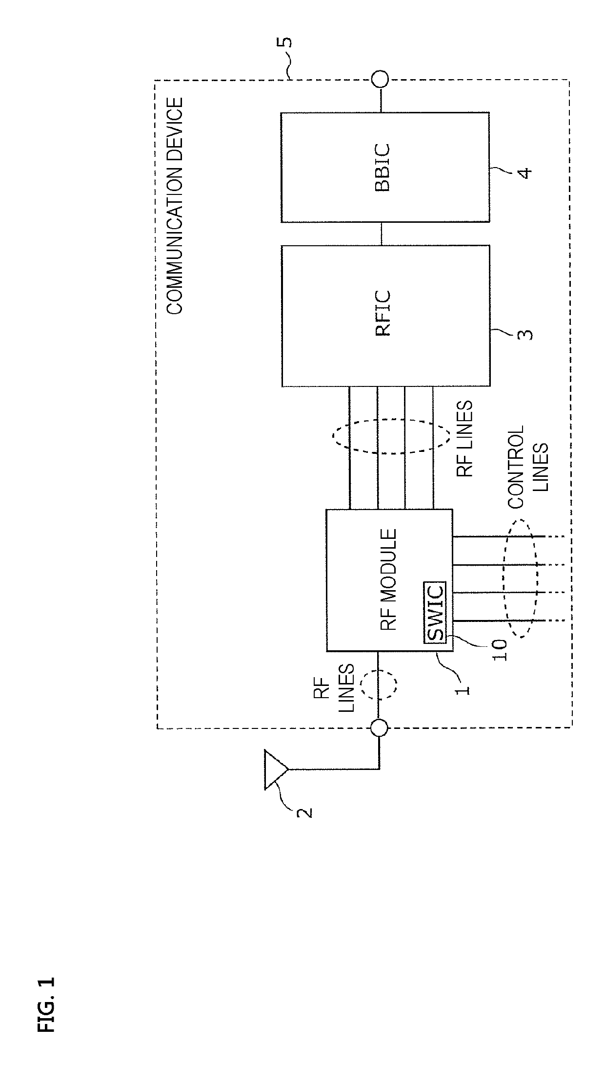
[0036]A high-frequency module (RF module) 1 according to a Preferred Embodiment 1 of the present invention is included in a communication device 5 used to transmit and receive a high-frequency signal, for example.
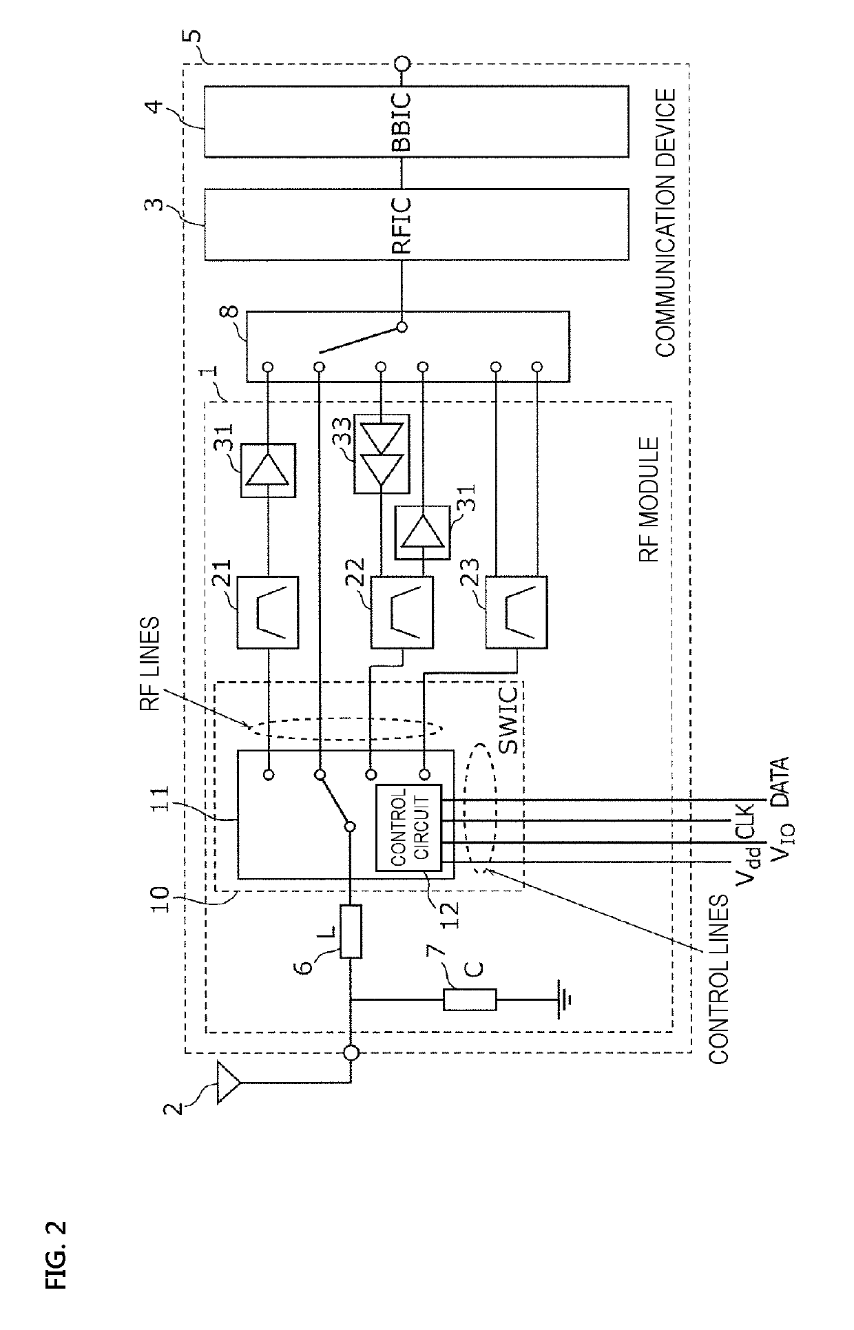
[0037]First, a configuration of the communication device 5 according to the present preferred embodiment will be described. FIG. 1 is a functional block diagram of the communication device 5 according to the present preferred embodiment. FIG. 2 is a schematic plan view illustrating a circuit configuration of the communication device 5 according to the present preferred embodiment.
[0038]As illustrated in FIG. 1 and FIG. 2, the communication device 5 includes the RF module 1, an RF signal processing circuit (RFIC) 3, and a basebandsignal processing circuit (BBIC) 4. The communication device 5 is connected to an antenna element 2. Note that, as illustrated in FIG. 2, the communication device 5 may include a switch 8 between the RF module 1 and the RFIC 3...
embodiment 2
Preferred Embodiment 2
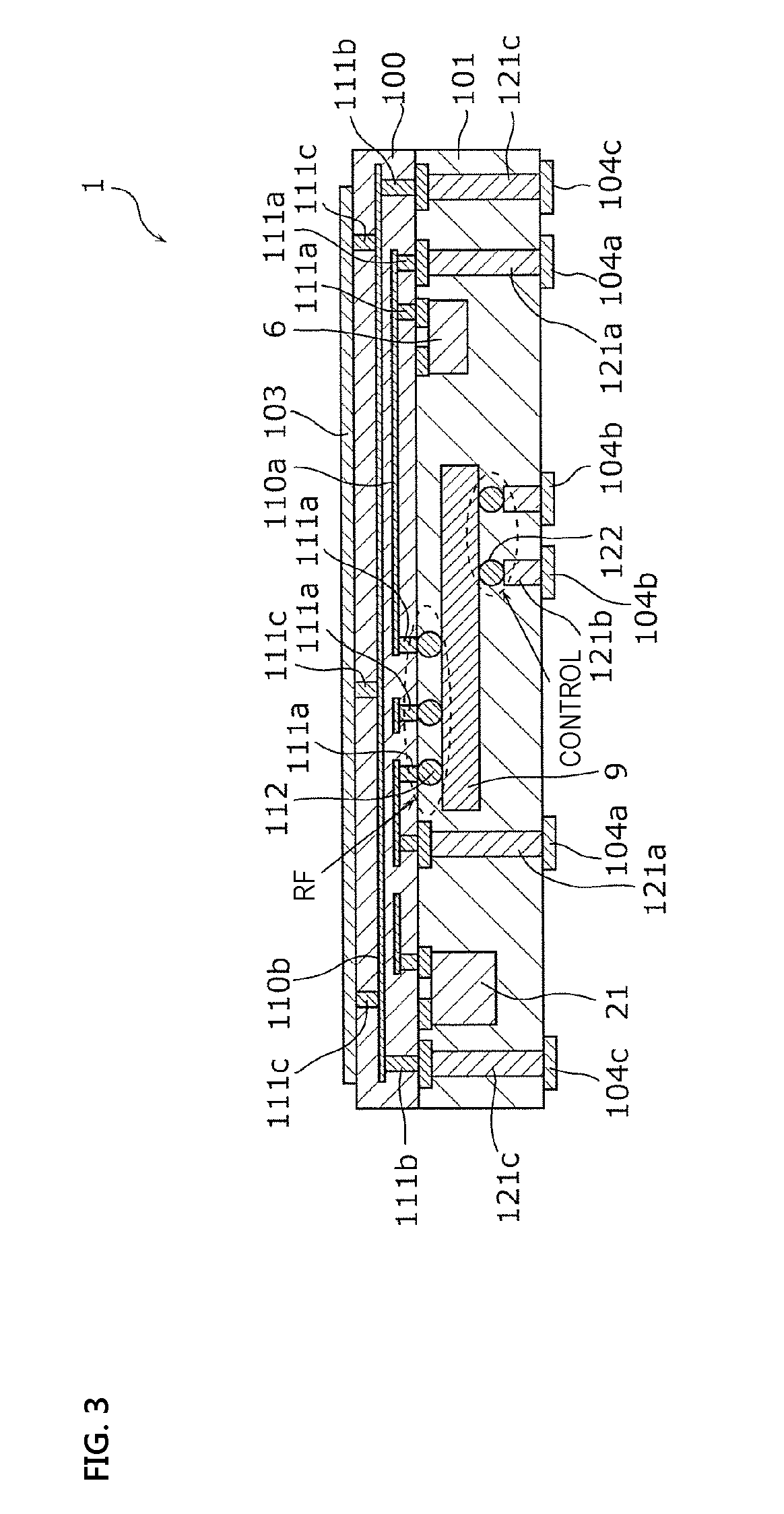
[0077]Next, an RF module 200 according to a Preferred Embodiment 2 of the present invention will be described. FIG. 6 is a sectional view illustrating a configuration of the RF module 200 according to the present preferred embodiment.
[0078]The RF module 200 according to the present preferred embodiment is different from the RF module 1 according to the Preferred Embodiment 1 in that electronic components are mounted on both sides of the circuit board 100, and sealed with a resin 201. Further, a shield 203 is provided on a top surface and side surfaces of the RF module 200. Here, the top surface of the RF module 200 refers to a surface opposite to a surface on which the outer electrodes 104a, 104b, and 104c are provided in the RF module 200. Further, the side surfaces refer to surfaces that connect the top surface and the surface of the RF module 200 on which the outer electrodes 104a, 104b, and 104c are provided.
[0079]As illustrated in FIG. 6, similar to the RF...
embodiment 3
Preferred Embodiment 3
[0086]Next, an RF module 300 according to a Preferred Embodiment 3 of the present invention will be described. FIG. 7 is a sectional view illustrating a configuration of the RF module 300 according to the present preferred embodiment.
[0087]The RF module 300 according to the present preferred embodiment is different from the RF module 200 according to the Preferred Embodiment 2 in that connection conductors 301 are provided in place of the shield 203 provided on the side surfaces in the RF module 200.
[0088]As illustrated in FIG. 7, similar to the RF module 200 described in the Preferred Embodiment 2, the RF module 300 includes the active element 9, the inductor 6, the capacitor 7 (not shown), the filters 21, 22, and 23 (not shown), the low-noiseamplifier 31 (not shown), and the power amplifier 33 (not shown), on a surface of the circuit board 100 on which the connection conductors 111a and 111b are exposed. These electronic components are sealed on the circuit ...
PUM
Abstract
A high-frequency module includes a circuit board including wiring patterns, a resin on an active element mounted on the circuit board and a side of the circuit board and sealing the active element, and connection conductors penetrating the resin from a surface of the resin and provided on a top surface of the active element. The active element includes a first connection electrode on a surface facing the circuit board, and a second connection electrode on a top surface opposite to the surface facing the circuit board. The first connection electrode is connected to a wiring pattern on the circuit board, and the second connection electrode is connected to the connection conductor and an outer electrode and is not connected to the wiring pattern.
Description
CROSS REFERENCE TO RELATED APPLICATIONS[0001]This application claims the benefit of priority to Japanese Patent Application No. 2016-243801 filed on Dec. 15, 2016 and is a Continuation Application of PCT Application No. PCT / JP2017 / 044417 filed on Dec. 11, 2017. The entire contents of each of these applications are hereby incorporated herein by reference.BACKGROUND OF THE INVENTION1. Field of the Invention[0002]The present invention relates to an active element, a high-frequency module, and a communication device.2. Description of the Related Art[0003]In recent years, as a method for controlling a switch provided in a high-frequency module, such as a high-frequency front end circuit, switch control using digital signals is becoming mainstream. In the switch control using digital signals, a digital controlsignal, which is a pulsed serial clocksignal, is supplied to a control circuit of a switch and an amplifier circuit to drive the switch and the amplifier circuit. In such a high-fr...
Claims
Application Information
Patent Timeline
Application Date:The date an application was filed.
Publication Date:The date a patent or application was officially published.
First Publication Date:The earliest publication date of a patent with the same application number.
Issue Date:Publication date of the patent grant document.
PCT Entry Date:The Entry date of PCT National Phase.
Estimated Expiry Date:The statutory expiry date of a patent right according to the Patent Law, and it is the longest term of protection that the patent right can achieve without the termination of the patent right due to other reasons(Term extension factor has been taken into account ).
Invalid Date:Actual expiry date is based on effective date or publication date of legal transaction data of invalid patent.

