
Combining simulation and optical microscopy to determine inspection mode

a technology of optical microscopy and simulation, applied in the direction of image enhancement, image analysis, instruments, etc., can solve the problems of difficult determining the best optical inspection mode, long time-consuming, complicated and time-consuming to find defect examples, etc., and achieve the effect of optimizing signal-to-noise characteristics

Active Publication Date: 2019-09-19
KLA TENCOR TECH CORP
View PDF8 Cites 7 Cited by
  • Summary
  • Abstract
  • Description
  • Claims
  • Application Information

AI Technical Summary

Benefits of technology

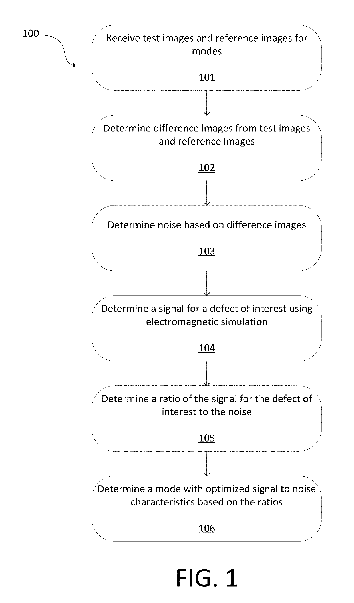
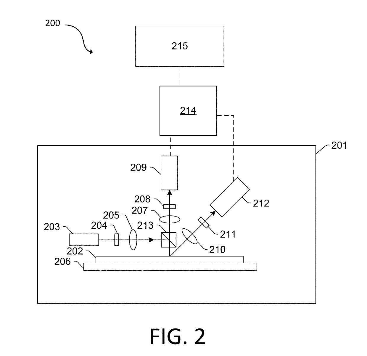
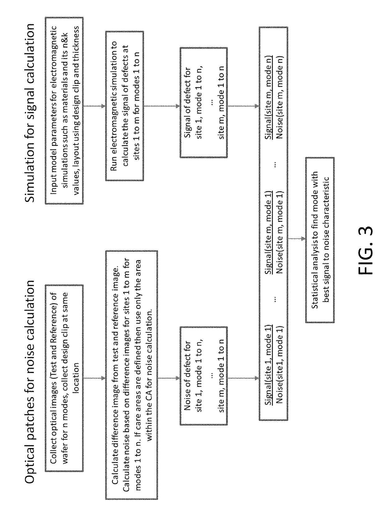
The patent text describes a system and method for detecting defects on semiconductor wafers using a light source and a detector. The system collects test images of the wafer and reference images for multiple modes. The processor then calculates difference images and use electromagnetic simulation to determine the signal for a defect of interest at various sites and modes. The system also analyzes ratios to identify the best site and mode for detecting defects. These ratios correspond to a maximum signal-to-noise characteristic. The method can adjust the system to use the optimized mode. The technical effect of this patent is to provide a more accurate and reliable system for detecting defects on semiconductor wafers.

Problems solved by technology

Finding gap defects is complicated and time-consuming.
If the defect density is low, it can take a long time to find defect examples by running hot scans or relying on electron beam tools.
Determining a best optical inspection mode can be challenging when there are not enough defects of interest (DOIs) in a sample because there are not statistics to properly evaluate the optical inspection mode.
Determining a best optical inspection mode also can be challenging when there are insufficient examples of noise.
Simulating noise is difficult because the noise source is not known.
This means a model cannot be created to simulate noise because what the noise / nuisance actually looks like is not known.
However, this simulation-based approach often fails to create a correct model of the noise structure.
It is generally difficult to create a proper model of the noise and requires a substantial time investment.
Typically only a subset of noise sources can be identified and the predictions frequently are wrong because the noise source is not known.
The optics selector can fail when there are no DOI or only a few DOI available, which is often the case.
Determining what the limiting noise source is and how to model the noise is generally difficult to perform properly.
Furthermore, optical mode selection on the tool can only be performed efficiently when defect examples are available, which is often not the case for a gap defect.

Method used


Image

  • Combining simulation and optical microscopy to determine inspection mode
  • Combining simulation and optical microscopy to determine inspection mode
  • Combining simulation and optical microscopy to determine inspection mode

Examples


Embodiment Construction

[0024]Although claimed subject matter will be described in terms of certain embodiments, other embodiments, including embodiments that do not provide all of the benefits and features set forth herein, are also within the scope of this disclosure. Various structural, logical, process step, and electronic changes may be made without departing from the scope of the disclosure. Accordingly, the scope of the disclosure is defined only by reference to the appended claims.

[0025]Embodiments disclosed herein can find a best optical inspection mode to detect defects when no defect examples or only a limited number of defect examples are available. Examples of noise on a tool can be used with DOI from simulations. An example of a DOI on the wafer is not required, which saves time and effort. Time and effort-intensive study of possible noise sources can be avoided because electromagnetic simulations and the DOI signal are used. Embodiments disclosed herein can deliver more accurate signal-to-no...


PUM


Abstract

A best optical inspection mode to detect defects can be determined when no defect examples or only a limited number of defect examples are available. A signal for a defect of interest at the plurality of sites and for the plurality of modes can be determined using electromagnetic simulation. A ratio of the signal for the defect of interest to the noise at each combination of the plurality of sites and the plurality of modes can be determined. A mode with optimized signal-to-noise characteristics can be determined based on the ratios.

Description

CROSS-REFERENCE TO RELATED APPLICATIONS[0001]This application claims priority to the provisional patent application filed Mar. 13, 2018 and assigned U.S. App. No. 62 / 642,161, the disclosure of which is hereby incorporated by reference.FIELD OF THE DISCLOSURE[0002]This disclosure relates to determining an optical inspection mode.BACKGROUND OF THE DISCLOSURE[0003]Evolution of the semiconductor manufacturing industry is placing greater demands on yield management and, in particular, on metrology and inspection systems. Critical dimensions continue to shrink, yet the industry needs to decrease time for achieving high-yield, high-value production. Minimizing the total time from detecting a yield problem to fixing it determines the return-on-investment for a semiconductor manufacturer.[0004]Fabricating semiconductor devices, such as logic and memory devices, typically includes processing a semiconductor wafer using a large number of fabrication processes to form various features and multi...

Claims


Application Information

Patent Timeline
IPC IPC(8): G06T7/00
CPCG06T7/001G06T2207/30148G06T2207/20224G06T2207/30168G06T2207/10056G06T5/70G01N21/9501G01N21/8806
Inventor BRAUER, BJORN
Owner KLA TENCOR TECH CORP
Learn More