Radio frequency modules and modules for moving target detection

a radio frequency module and target detection technology, applied in the field of radio frequency modules, can solve problems such as the degradation of characteristics, the degradation of monolithic microwave integrated circuit characteristics, and the particular noise characteristics of mmi

Inactive Publication Date: 2003-01-09
RENESAS ELECTRONICS CORP
View PDF0 Cites 2 Cited by
  • Summary
  • Abstract
  • Description
  • Claims
  • Application Information

AI Technical Summary

Benefits of technology

[0007] Accordingly, it is another object of the present invention to provide a radio frequency module that includes an oscillator or an amplifier having excellent S / N characteristics.
[0008] Various forms of field effect transistors used in conventional radio frequency modules, typified by a HEMT, each have problems that make it difficult to fully meet objects of the present invention. In addition to a HEMT with an ordinary structure, a HEMT with a composite channel has been proposed. The HEMT with a composite channel serves an object of the present invention to achieve high current drivability and high breakdown voltage.
[0009] A field effect transistor according to the present invention is intended to prevent breakdown due to physical characteristics of its channel materials or to avoid a problem of increase in noise caused by the composite channel. In other words, the present invention is intended to avoid problems of the composite channel and achieve both high current drivability and high breakdown voltage.
[0019] The HEMT is a field effect transistor comprising a first semiconductor layer containing an impurity; and a second semiconductor layer having a smaller band gap than that of the first semiconductor layer, the first semiconductor layer and the second semiconductor layer being joined together to form a heterostructure, the second semiconductor layer containing substantially no impurity, and the second semiconductor layer or an interface of the heterostructure functioning as a channel region. A gate electrode is disposed on the side of the first semiconductor layer containing an impurity. A channel region formed by a plurality of semiconductor layers is referred to as a composite channel. As described above, this composite channel is useful in achieving high output. The band gap of a semiconductor layer of the composite channel on a side farther from a gate electrode is generally selected to be larger than that of a semiconductor layer on the gate electrode side.

Problems solved by technology

Problems in achieving the above are factors that cause degradation in characteristics of a monolithic microwave integrated circuit having an oscillator formed with the field effect transistor (hereinafter abbreviated to an oscillator MMIC), an amplifier MMIC, and the like.
Problems in achieving the above are factors that cause degradation in characteristics of a transmitter or a receiver having such an oscillator MMIC or an amplifier MMIC.
The oscillator MMIC particularly has a problem of degradation in noise characteristics, while the amplifier MMIC particularly has a problem of difficulty in achieving high output at its amplifying stage, especially at its final stage.
The amplifier MMIC also invites degradation in noise characteristics.

Method used


Image

  • Radio frequency modules and modules for moving target detection
  • Radio frequency modules and modules for moving target detection
  • Radio frequency modules and modules for moving target detection

Examples


Embodiment Construction

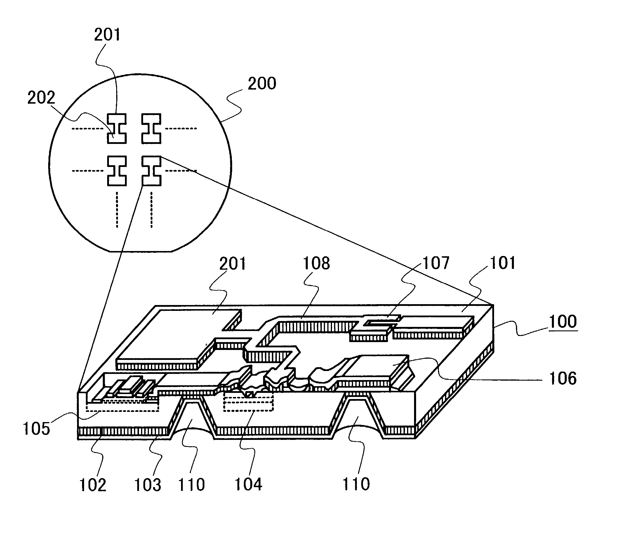
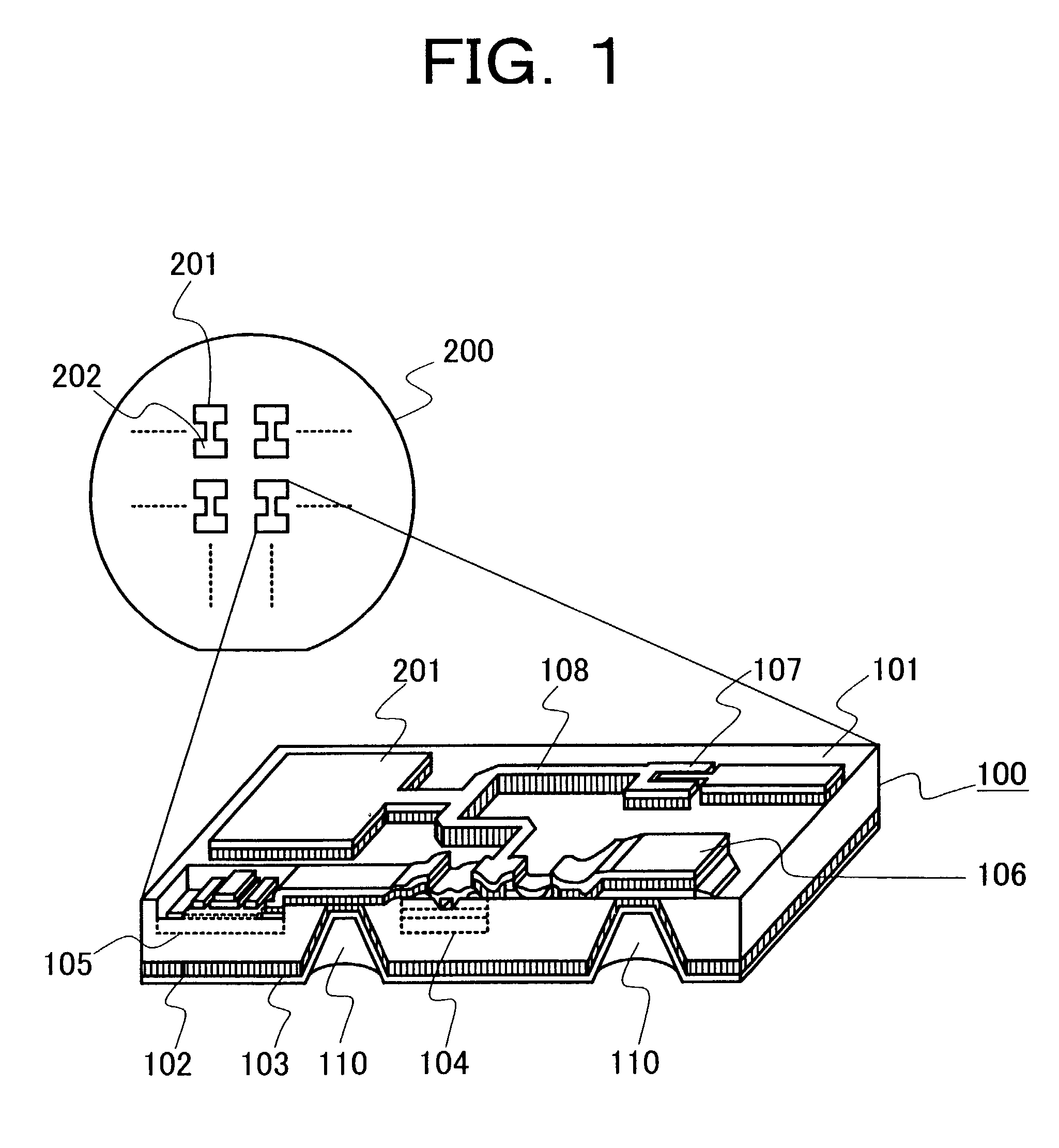
[0031] FIG. 1 shows a wafer 200 for forming an MMIC and a configuration example of the MMIC in perspective view. This example is one of a so-called microstrip type MMIC. Various microwave circuit devices are formed on a surface 101 of a semiconductor substrate 100, while a ground conductor 103 is formed on an underside 102 thereof. The semiconductor substrate 100 is formed by using a compound semiconductor of GaAs and InP, or Si, for example. Active devices such as a field effect transistor and a bipolar transistor as well as a resistance, a capacitance, an inductance, a transmission line or the like are formed on the surface of the semiconductor substrate. A grounding via-hole 110 is usually formed in the semiconductor substrate 100. An antenna 201 and a transceiver module 202 are illustrated in FIG. 1 as being in array arrangement on the wafer 200. FIG. 1 also illustrates a field effect transistor 104, an HBT (Hetero Bipolar Transistor) 105, a capacitor 106, an interdigital capaci...


PUM


Abstract

It is an object of the present invention to provide a radio frequency module incorporating an MMIC that has a high S / N ratio while ensuring a high output. A radio frequency module according to the present invention incorporates an MMIC having a field effect transistor in which channel layers for traveling of carriers are formed by a heterostructure of two or more different kinds of materials, and height of a potential barrier of an interface between the different kinds of materials is less than 0.22 eV.

Description

[0001] 1. Field of the Invention[0002] The present invention relates to a radio frequency module. The present invention relates particularly to a radio frequency module incorporating a monolithic microwave integrated circuit (hereinafter abbreviated to an MMIC) fabricated by using a field effect transistor capable of achieving a high S / N ratio. More particularly, the present invention relates to a field effect transistor that can achieve a high S / N ratio. Still more particularly, the present invention relates to a module for moving target detection.[0003] 2. Related Arts[0004] For a radio frequency module, especially a module required to provide a high output, the following techniques are employed. For high output, there is known a technique in which a high electron mobility transistor, commonly referred to as a HEMT, which has a channel layer of high indium content is used in an MMIC including an amplifier (hereinafter abbreviated to an amplifier MMIC). This technique is intended t...

Claims


Application Information

Patent Timeline
Patent Type & Authority Applications(United States)
IPC IPC(8): H01L27/04H01L27/06H01L29/778H01L21/822H01L29/812
CPCH01L27/0605H01L29/7783H01L29/812
Inventor HIGUCHI, KATSUHIKOTAKATANI, SHINICHIRO
Owner RENESAS ELECTRONICS CORP
Why Eureka
Try Eureka