
Solid-state imaging device, control method thereof, and electronic apparatus

Active Publication Date: 2019-09-19
SONY SEMICON SOLUTIONS CORP
View PDF4 Cites 5 Cited by
  • Summary
  • Abstract
  • Description
  • Claims
  • Application Information

AI Technical Summary

Benefits of technology

The present technology allows for adjusting the operation range of a differential amplifier to optimize its performance. This results in improved efficiency and accuracy of signal processing. The technology can be used in various applications where signal amplification and processing are necessary.

Problems solved by technology

If the amplification rate is large, there is an effect that an input-referred noise generated in the AD conversion unit at the subsequent stage becomes small.

Method used


Image

  • Solid-state imaging device, control method thereof, and electronic apparatus
  • Solid-state imaging device, control method thereof, and electronic apparatus
  • Solid-state imaging device, control method thereof, and electronic apparatus

Examples


first embodiment

[0048]1. Schematic configuration of solid-state imaging device

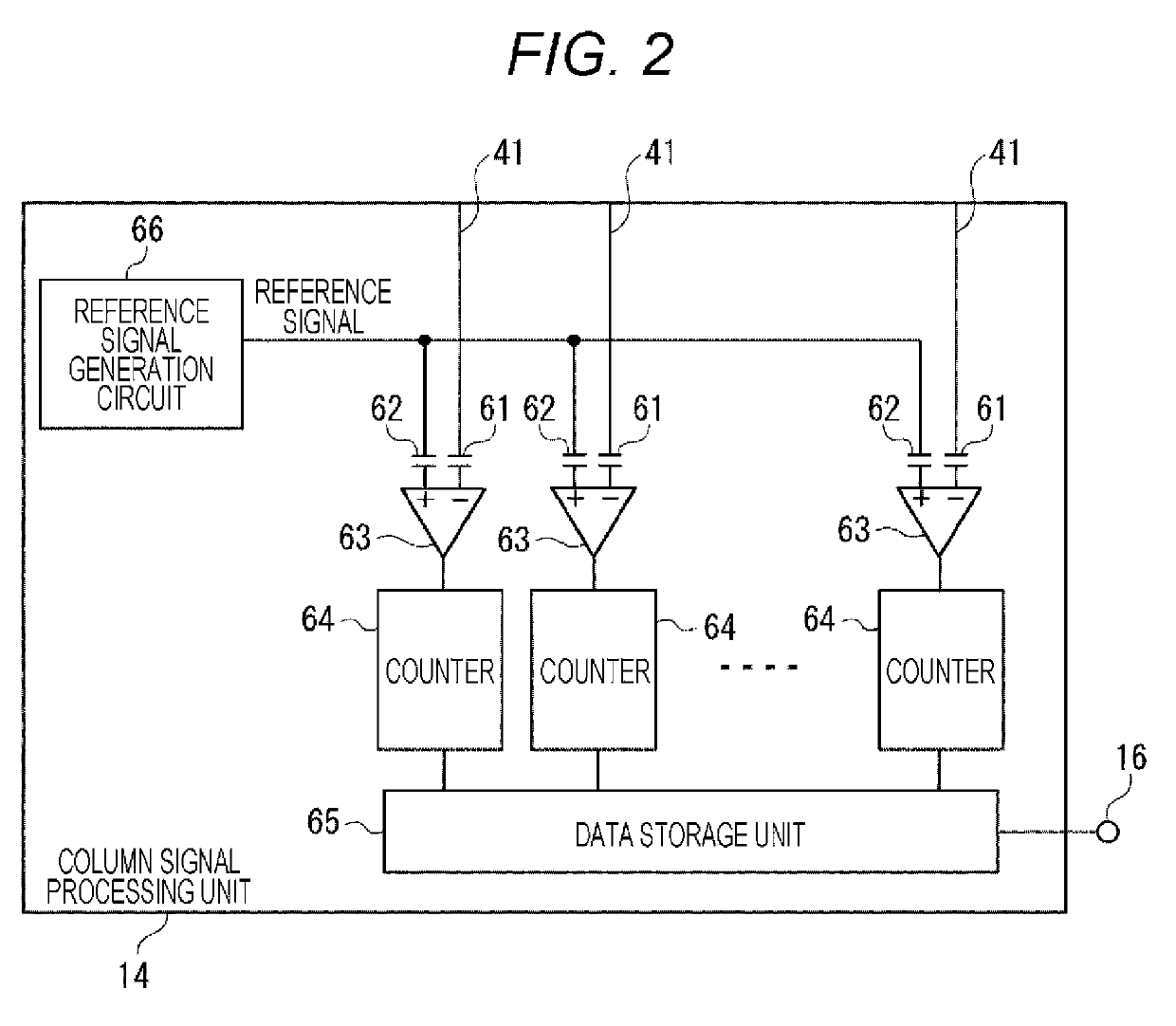
[0049]2. Configuration example of column signal processing unit

[0050]3. First configuration example of differential amplifier component

[0051]4. Second configuration example of differential amplifier component

[0052]5. Third configuration example of differential amplifier component

[0053]6. Fourth configuration example of differential amplifier component

[0054]7. Fifth configuration example of differential amplifier component

[0055]8. Sixth configuration example of differential amplifier component

[0056]9. Seventh configuration example of differential amplifier component

[0057]10. Eighth configuration example of differential amplifier component

[0058]11. Ninth configuration example of differential amplifier component

[0059]12. Tenth configuration example of differential amplifier component

[0060]13. Eleventh configuration example of differential amplifier component

[0061]14. Twelfth configuration example of differential amplifier co...

second embodiment

[0065]18. Schematic configuration of solid-state imaging device of second embodiment

[0066]19. Configuration example of signal switching unit

[0067]20. Summary

[0068]21. Application Example of Electronic Apparatus>

[0069]

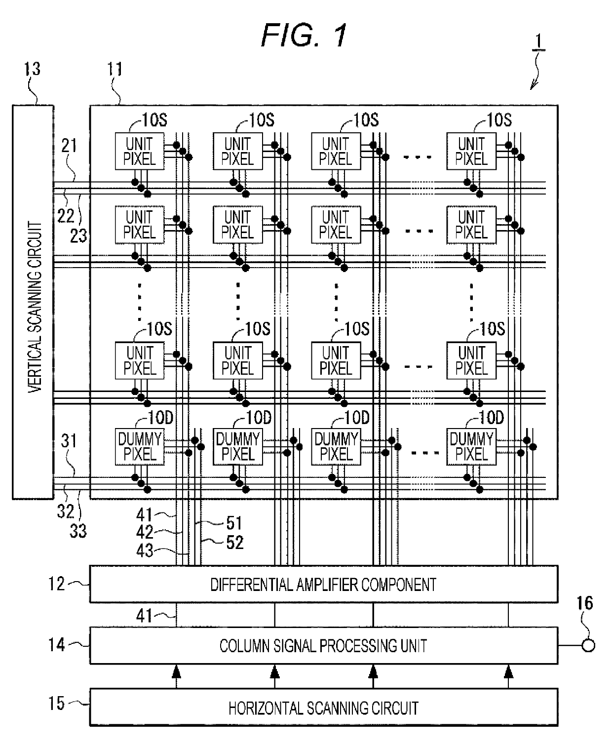
[0070]FIG. 1 is a diagram showing a schematic configuration of a solid-state imaging device (a CMOS image sensor) according to a first embodiment of the present technology.

[0071]A solid-state imaging device 1 of FIG. 1 includes a pixel array unit 11, a differential amplifier component 12, a vertical scanning circuit 13, a column signal processing unit 14, a horizontal scanning circuit 15, and the like which are formed on, for example, a semiconductor substrate using Si (silicon) as a semiconductor.

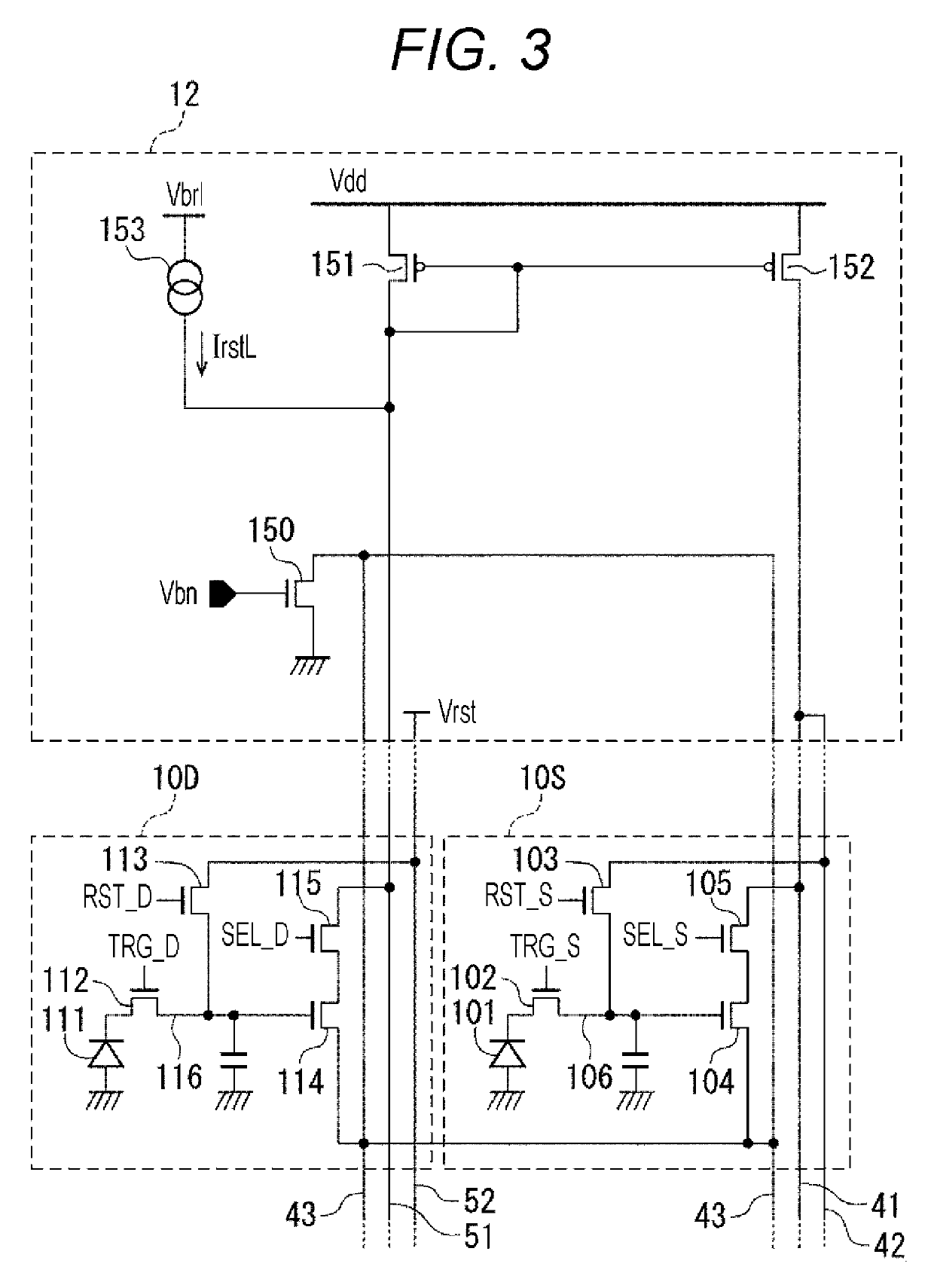
[0072]The pixel array unit 11 is provided with a unit pixel 10S and a dummy pixel 10D. Specifically, the unit pixels 10S are arranged in an array inside an effective pixel area of the pixel array unit 11 and one dummy pixel 10D is disposed in at least one pixel column outside ...


PUM


Abstract

An imaging device includes a plurality of pixels including a first pixel and a second pixel, and a differential amplifier including a first amplification transistor, a second amplification transistor, and a first load transistor. The first load transistor receives a power source voltage. The imaging device includes a first signal line coupled to the first amplification transistor and the first load transistor, a second signal line coupled to the second amplification transistor, and a first reset transistor configured to receive the power source voltage. A gate of the first reset transistor is coupled to the first load transistor. The first pixel includes a first photoelectric conversion element and the first amplification transistor, and the second pixel includes a second photoelectric conversion element and the second amplification transistor.

Description

TECHNICAL FIELD[0001]The present technology relates to a solid-state imaging device, a control method thereof, and an electronic apparatus and more particularly to a solid-state imaging device capable of adjusting an operation range of a differential amplifier within an optimal operation range, a control method thereof, and an electronic apparatus.CROSS REFERENCE TO RELATED APPLICATIONS[0002]This application claims the benefit of Japanese Priority Patent Application JP 2016-209290 filed on Oct. 26, 2016, the entire contents of which are incorporated herein by reference.BACKGROUND ART[0003]A solid-state imaging device has, for example, a configuration in which a photodiode (PD) corresponding to a photoelectric conversion element, four pixel transistors including a transfer transistor, a reset transistor, an amplification transistor, and a selection transistor, and a floating diffusion (FD) are disposed at each pixel. In each pixel, a signal charge which is photoelectrically converted...

Claims


Application Information

Patent Timeline
IPC IPC(8): H04N5/3745H04N5/357H04N5/378
CPCH04N5/357H04N5/3745H04N5/378H04N25/60H04N25/77H04N25/75
Inventor ZHU, HONGBOSATO, MAMORUKATO, AKIHIKO
Owner SONY SEMICON SOLUTIONS CORP
Features
  • Generate Ideas
  • Intellectual Property
  • Life Sciences
  • Materials
  • Tech Scout
  • Unparalleled Data Quality
  • Higher Quality Content
  • 60% Fewer Hallucinations
Learn More