Light-emitting device with mixed nanoparticle charge transport layer

a charge transport layer and light-emitting device technology, applied in the direction of solid-state devices, organic semiconductor devices, material nanotechnology, etc., can solve the problems of inability to optimize the charge mobility to match etl electron injection and htl hole injection, and the fixed mobility of etl for a given nanoparticle material configuration, etc., to achieve a larger tunability range and effective

Active Publication Date: 2019-09-26
SHARP KK
View PDF7 Cites 6 Cited by
  • Summary
  • Abstract
  • Description
  • Claims
  • Application Information

AI Technical Summary

Benefits of technology

[0009]To provide a robust charge transfer layer with a specific charge mobility, embodiments of the present invention include a light-emitting device structure with a novel charge transfer layer comprised of a mixture of at least two different populations of nanoparticles, in which the two different populations of nanoparticles differ in the energetic alignment of either or both of their conduction band or valence band edge. Such a combination of nanoparticles provides an effective resistance that is not a simple average of their individual resistances, but provides a much larger range of tunability, due to the method of conduction that occurs in a nanoparticle matrix. The different populations of nanoparticles may be energetically non-aligned by being made of different materials, or by being particles of different sizes or shapes of a same or similar material.

Problems solved by technology

Such a configuration, however, has a deficiency in that the ETL has a fixed mobility for a given nanoparticle material configuration.
Even using such teachings, however, optimization of charge mobility to match ETL electron injection and HTL hole injection has not been achieved.

Method used


Image

  • Light-emitting device with mixed nanoparticle charge transport layer
  • Light-emitting device with mixed nanoparticle charge transport layer
  • Light-emitting device with mixed nanoparticle charge transport layer

Examples


Embodiment Construction

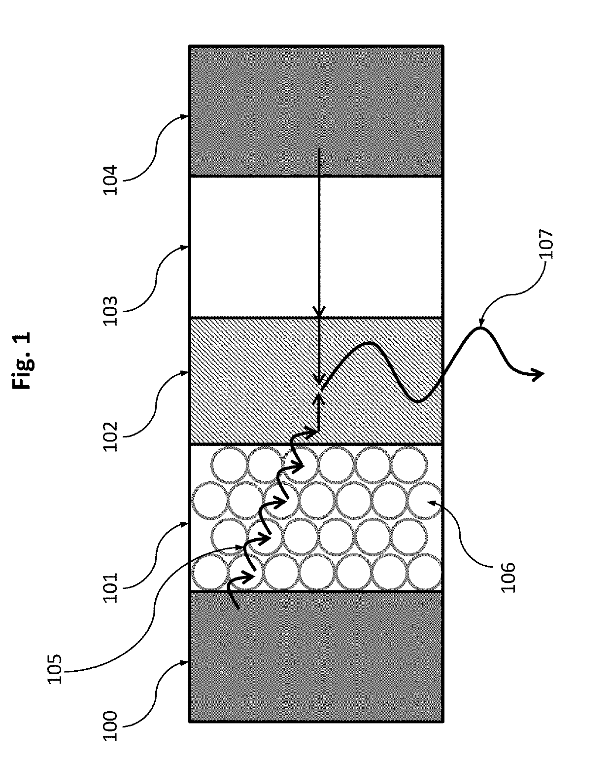
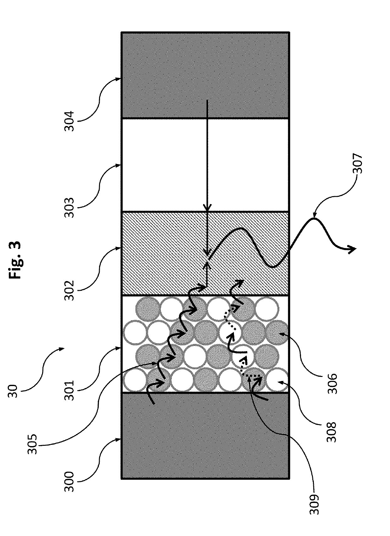
[0025]Embodiments of the present invention will now be described with reference to the drawings, wherein like reference numerals are used to refer to like elements throughout. It will be understood that the figures are not necessarily to scale.

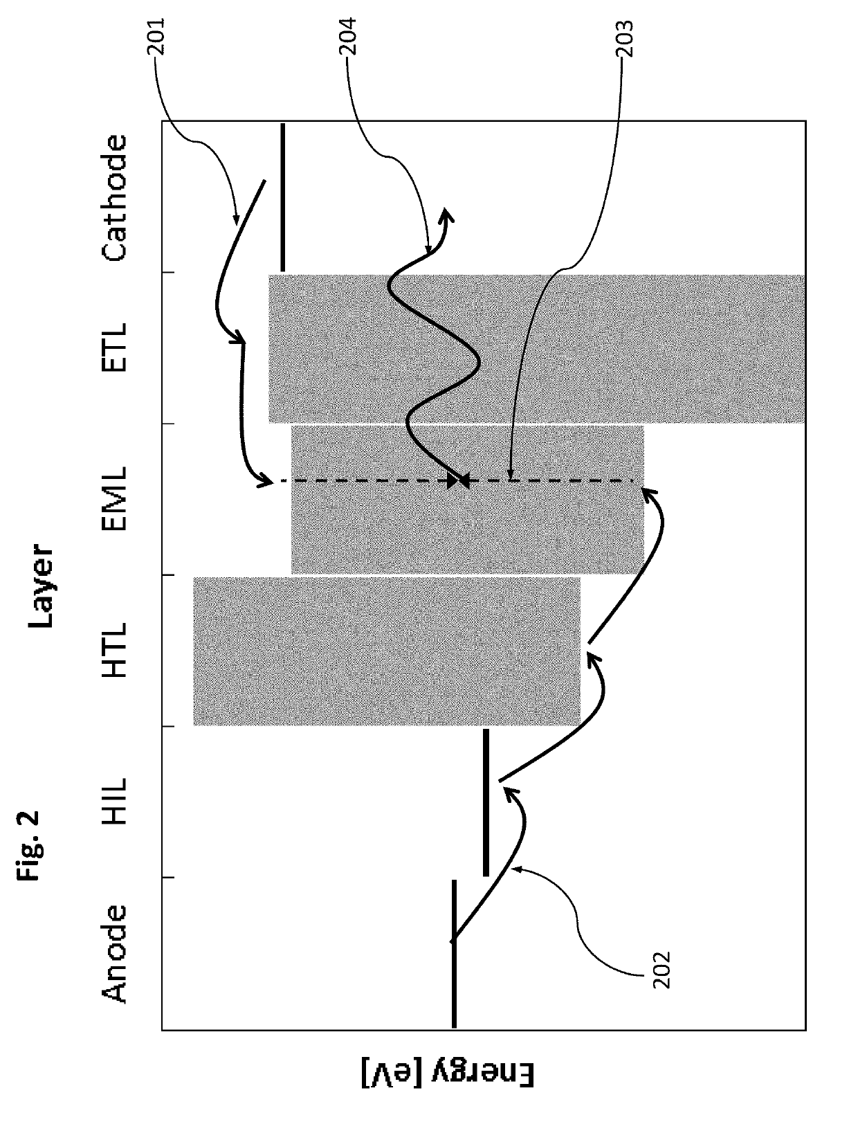
[0026]To provide a robust charge transfer layer with a specific charge mobility, embodiments of the present invention include a light-emitting device structure with a novel charge transfer layer comprised of a mixture of at least two different populations of nanoparticles, in which the two different populations of nanoparticles differ in the energetic alignment of either or both of their conduction band or valence band edge. Such a combination of nanoparticles provides an effective resistance that is not a simple average of their individual resistances, but provides a much larger range of tunability, due to the method of conduction that occurs in a nanoparticle matrix. The different populations of nanoparticles may be energetically non-aligned...


PUM


Abstract

A light-emitting device is optimized for radiative recombination and minimizes non-radiative recombination. The light-emitting device includes an emissive layer, a first electrode and a second electrode from which charges are generated, a first charge transport layer that injects charges from the first electrode into the emissive layer, and a second charge transport layer that injects charges from the second electrode into the emissive layer. At least one of the charge transport layers includes a mixture of a first nanoparticle population and a second nanoparticle population, and the first nanoparticle population and the second nanoparticle population are conductive nanoparticles that are energetically non-aligned as between the first nanoparticle population and the second nanoparticle population. Nanoparticles of the first nanoparticle population and the second nanoparticle population are energetically non-aligned with each other by being made of different materials, by having nanoparticles of different sizes, and/or by having nanoparticles of different shapes.

Description

TECHNICAL FIELD[0001]The present invention relates to light-emitting devices including inorganic nanoparticle layers for charge transport, and more particularly to devices in which an inorganic nanoparticle layer acts as a charge transport layer in a light-emitting device.BACKGROUND ART[0002]An example of a conventional light-emitting device is described in U.S. Pat. No. 9,525,148 (Kazlas et al., issued Dec. 20, 2016). FIG. 1 is a drawing depicting an exemplary representation of such a conventional light-emitting device. A conventional light-emitting device includes an anode 104 and cathode 100, and a light-emitting layer 102 containing a material that emits light 107. Within the light-emitting layer 102, light is produced upon electron and hole recombination to generate the light 107. The light-emitting layer 102 may be an inorganic or organic semiconductor layer, or a layer of quantum dots (QDs). At least one hole transport layer 103 is located between the anode 104 and the emissi...

Claims


Application Information

Patent Timeline
Patent Type & Authority Applications(United States)
IPC IPC(8): H01L51/50
CPCH01L51/502H01L51/5056H01L51/5072H01L2251/303H01L51/5004H01L2251/5369B82Y30/00H10K50/16H10K50/15H10K2102/00H10K71/00H10K50/11H10K2101/40H10K50/115H10K2102/331
Inventor PALLES-DIMMOCK, JAMES ANDREW ROBERTBOARDMAN, EDWARD ANDREWSMEETON, TIM MICHAEL
Owner SHARP KK
Why Eureka
Try Eureka