Display device and method for driving the same

Active Publication Date: 2019-10-24
SHARP KK
View PDF3 Cites 1 Cited by
  • Summary
  • Abstract
  • Description
  • Claims
  • Application Information

AI Technical Summary

Benefits of technology

[0008]Accordingly, it is an object of the following disclosure to achieve a display device including a

Problems solved by technology

However, each source bus line cannot transmit the video signal indicating the pixel voltage values for a plurality of rows at one time (simultaneously).
However, as a size and definition of the panel are bei

Method used


Image

  • Display device and method for driving the same
  • Display device and method for driving the same
  • Display device and method for driving the same

Examples


first embodiment

1. First Embodiment

1.1 Relationship Between Positions of Direct Current Voltage Input Terminals and Vertical Scanning Direction

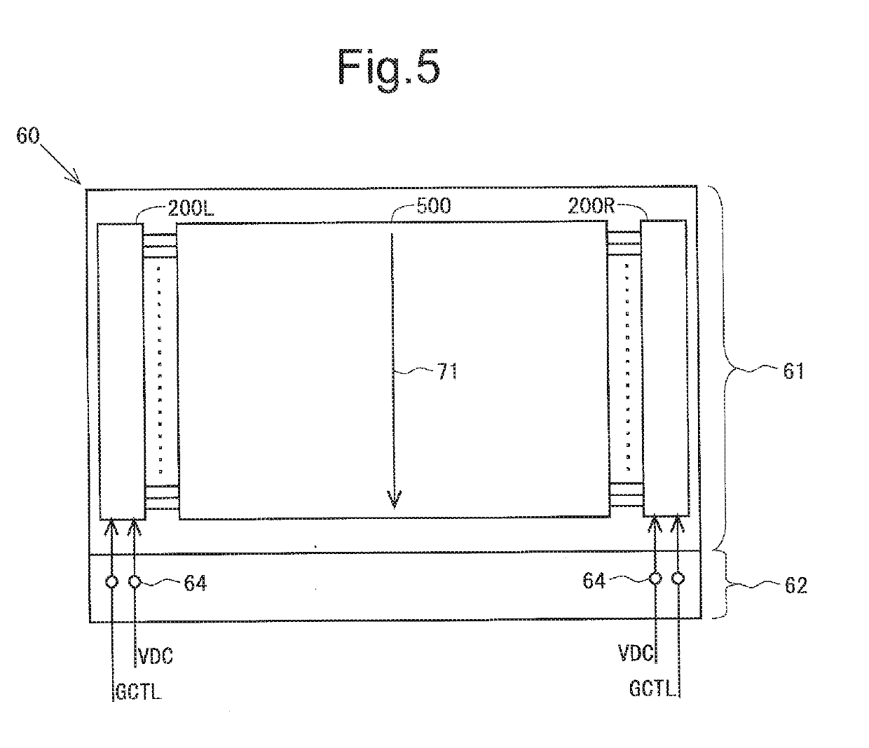
[0069]A description will be made of a relationship between positions of direct current voltage input terminals 64 and a vertical scanning direction with reference to FIG. 5. A liquid crystal panel 60 that constitutes the liquid crystal display device includes two glass substrates. One of the glass substrates is called an array substrate, and the other of the glass substrates is called a counter substrate. The array substrate and the counter substrate are pasted to each other, for example, by a sealing material. An area of the array substrate is larger than an area of the counter substrate. Hence, in a region on the array substrate, there is a picture-frame region 62 that is a region that does not face the counter substrate. Note that, in the present specification, a region where the array substrate and the counter substrate completely face each other (a regi...

third modified example

1.5.3 Third Modified Example

[0108]FIG. 16 is a diagram for explaining a relationship between positions of direct current voltage input terminals and the vertical scanning direction in the present modified example. In the present modified example, as illustrated in FIG. 16, a picture-frame region 62u is provided above the active region 61, and a picture-frame region 62d is provided below the active region 61. Then, direct current voltage input terminals 64u are provided on the vertical scanning start side on the liquid crystal panel 60, and direct current voltage input terminals 64d are provided on the vertical scanning end side on the liquid crystal panel 60. That is, the direct current voltage VDC is inputted to the gate drivers 200L and 200R from both of the vertical scanning start side and the vertical scanning end side. According to the present modified example, the voltage drop of the direct current voltage VDC is smallest on the vertical scanning start side and the vertical sc...

fourth modified example

1.5.4 Fourth Modified Example

[0110]FIG. 19 is a circuit diagram illustrating a configuration of a unit circuit 2 in the present modified example. In the first embodiment, the thin film transistor T3 composes the diode connection. In contrast, a thin film transistor T3 in the present modified example is connected at its gate terminal to the input terminal 23, connected at its drain terminal to the input terminal 21, and connected at its source terminal to the first node NA. That is, the drain terminal of the thin film transistor T3 is given the direct current voltage VDC. Also by such a configuration, each unit circuit 2 operates similarly to that in the first embodiment. Hence, also in the present modified example, variation in the magnitude of the scanning voltage among the gate bus lines GL is reduced, and the unevenness in display is suppressed from occurring.


PUM


Abstract

There is adopted a gate driver with a system of applying a direct current voltage as an active scanning signal to a gate bus line through a buffer transistor in a unit circuit that composes a shift register, and a display device is provided with a direct current voltage generation circuit that generates the direct current voltage. The direct current voltage generation circuit changes a voltage level of the direct current voltage in each frame period. For example, when a direct current voltage input terminal is provided on a vertical scanning end side, the direct current voltage generation circuit gradually decreases the voltage level of the direct current voltage in each frame period.

Description

BACKGROUND OF THE INVENTION1. Field of the Invention[0001]The following disclosure relates to a display device including a monolithic gate driver with a system in which a direct current voltage is applied as an active scanning signal to a gate bus line (scanning signal line) via a transistor in a shift register, and to a method for driving the display device.2. Description of Related Art[0002]Heretofore, there has been known an active matrix type liquid crystal display device provided with a display unit including a plurality of source bus lines (video signal lines) and a plurality of gate bus lines. With regard to such a liquid crystal display device, heretofore, in many cases, a gate driver (scanning signal line drive circuit) for driving the gate bus lines has been mounted as an integrated circuit (IC) chip on a peripheral portion of a substrate that constitutes a liquid crystal panel. However, in recent years, in order to narrow a frame of the liquid crystal display device, it h...

Claims


Application Information

Patent Timeline
IPC IPC(8): G09G3/36
CPCG09G2320/0233G11C19/28G09G3/3677G09G2310/0286G09G3/3696G09G3/3674G09G2300/0408G09G2330/021
Inventor TAGAWA, AKIRAIWASE, YASUAKIWATANABE, TAKUYAKUSUMI, TAKATSUGUTAKEUCHI, YOHEI
Owner SHARP KK
Why Eureka
Try Eureka