Image sensor with boosted photodiodes for time of flight measurements

a technology of image sensor and photodiode, applied in the field of semiconductor devices, can solve the problems of large computer processing power, difficult to create 3d images using small devices, complex techniques,

Active Publication Date: 2019-11-07
OMNIVISION TECH INC
View PDF0 Cites 10 Cited by
  • Summary
  • Abstract
  • Description
  • Claims
  • Application Information

AI Technical Summary

Problems solved by technology

One disadvantage with this triangulation technique is that it is difficult to create 3D images using small devices because there must be a minimum separation distance between each camera in order to create the three dimensional images.
In addition, this technique is complex and therefore requires significant computer processing power in order to create the 3D images in real time.
A continuing challenge with t

Method used


Image

  • Image sensor with boosted photodiodes for time of flight measurements
  • Image sensor with boosted photodiodes for time of flight measurements
  • Image sensor with boosted photodiodes for time of flight measurements

Examples


Embodiment Construction

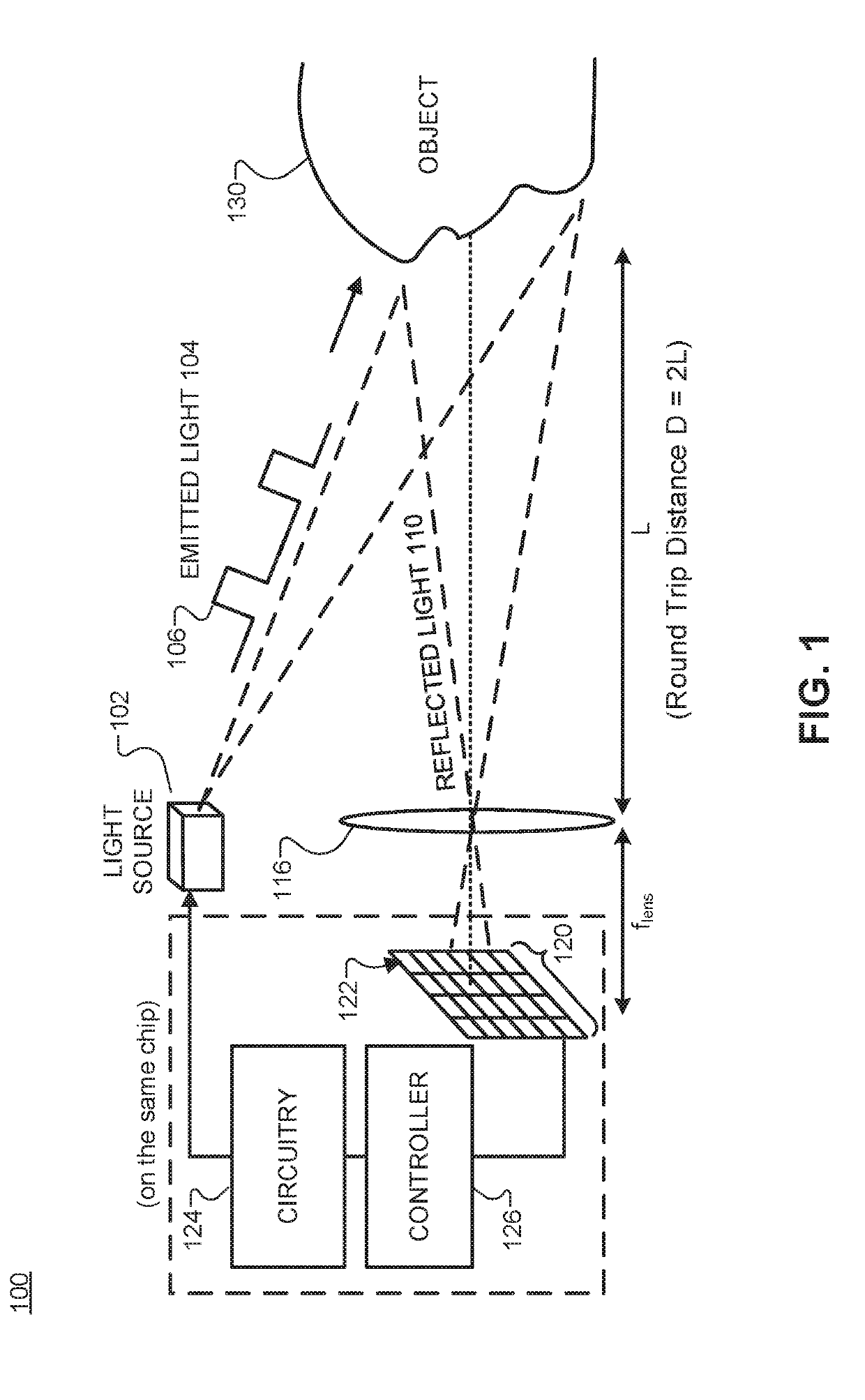
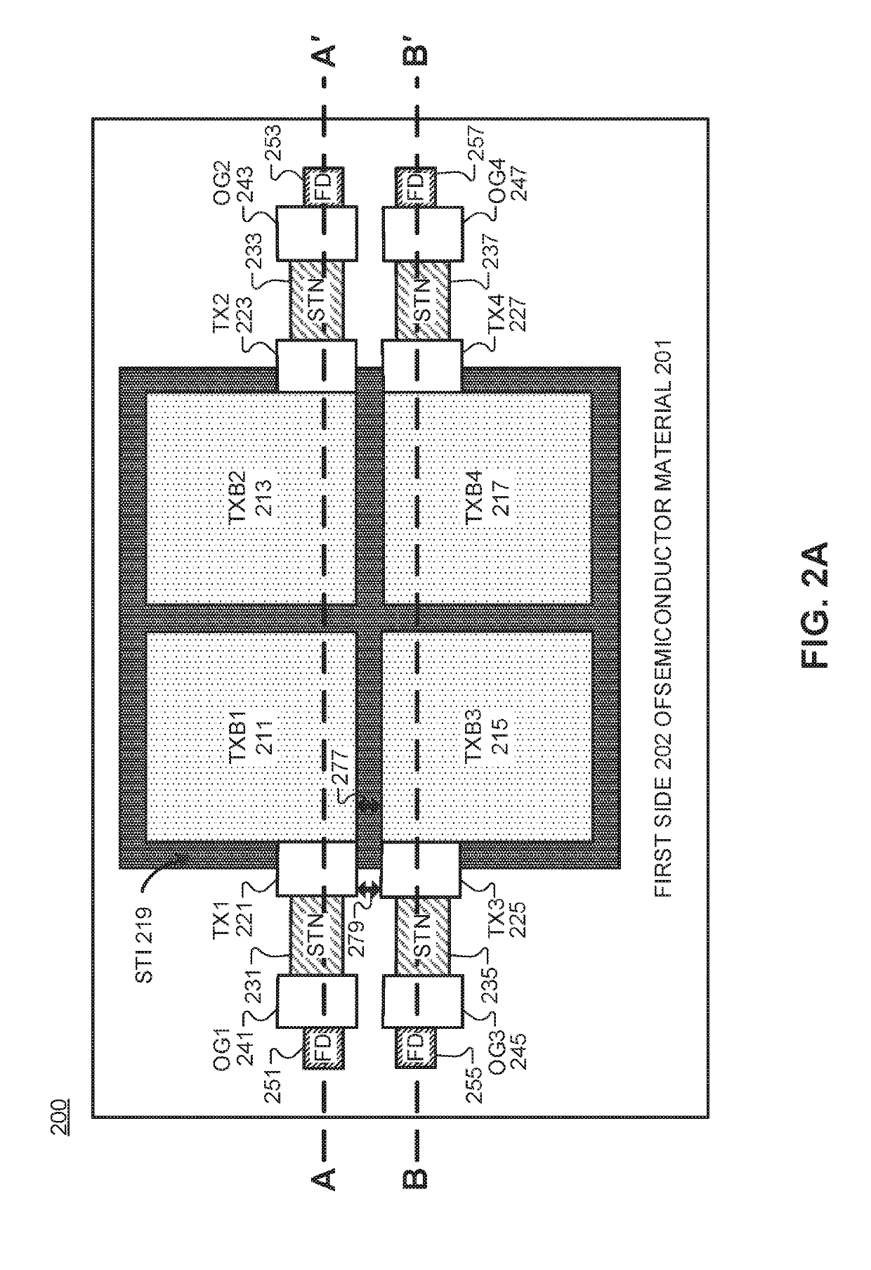
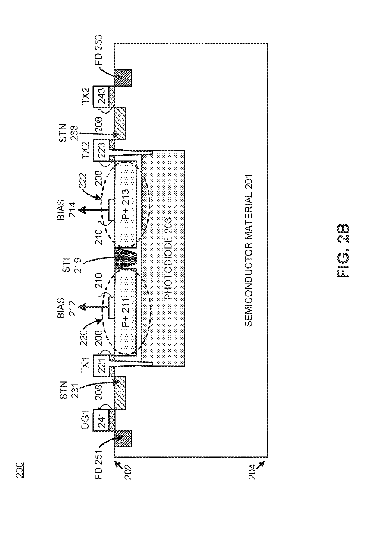
[0022]Examples of an apparatus, system, and method for an image sensor with boosted photodiodes for time of flight measurements are described herein. In the following description, numerous specific details are set forth to provide a thorough understanding of the examples. One skilled in the relevant art will recognize, however, that the techniques described herein can be practiced without one or more of the specific details, or with other methods, components, materials, etc. In other instances, well-known structures, materials, or operations are not shown or described in detail to avoid obscuring certain aspects.

[0023]Reference throughout this specification to “one example” or “one embodiment” means that a particular feature, structure, or characteristic described in connection with the example is included in at least one example of the present invention. Thus, the appearances of the phrases “in one example” or “in one embodiment” in various places throughout this specification are ...


PUM


Abstract

An image sensor including a photodiode, a first doped region, a second doped region, a first storage node, a second storage node, a first vertical transfer gate, and a second vertical transfer gate is presented. The photodiode is disposed in a semiconductor material to convert image light to an electric signal. The first doped region and the second doped region are disposed in the semiconductor material between a first side of the semiconductor material and the photodiode. The first doped region is positioned between the first storage node and the second storage node while the second doped region is positioned between the second storage node and the first doped region. The vertical transfer gates are coupled between the photodiode to transfer the electric signal from the photodiode to a respective one of the storage nodes in response to a signal.

Description

TECHNICAL FIELD[0001]This disclosure relates generally to semiconductor devices, and in particular but not exclusively, relates to time of flight image sensors.BACKGROUND INFORMATION[0002]Interest in three dimension (3D) cameras is increasing as the popularity of 3D applications continues to grow in areas such as imaging, movies, games, computers, user interfaces, facial recognition, object recognition, augmented reality, and the like. A typical passive way to create 3D images is to use multiple cameras to capture stereo or multiple images. Using the stereo images, objects in the images can be triangulated to create the 3D image. One disadvantage with this triangulation technique is that it is difficult to create 3D images using small devices because there must be a minimum separation distance between each camera in order to create the three dimensional images. In addition, this technique is complex and therefore requires significant computer processing power in order to create the ...

Claims


Application Information

Patent Timeline
IPC IPC(8): G01S17/89H01L27/146G01S7/486H04N5/378H04N13/254H04N5/374G01S7/4863G01S17/894
CPCG01S17/89H04N13/254H04N5/378G01S7/4863H04N5/3742H01L27/1463H01L27/14643H01L27/1461H01L27/14612H01L27/14634H04N25/70H04N25/75G01S17/894H04N25/533H04N25/53H04N25/778H04N25/771H04N25/767
Inventor MANABE, SOHEIMABUCHI, KEIJI
Owner OMNIVISION TECH INC
Why Eureka
Try Eureka