Pixel array substrate and driving method thereof

a technology of pixel array and substrate, which is applied in the direction of electrical equipment, semiconductor devices, instruments, etc., can solve the problems of serious affecting the quality of the display panel, the reduction of light extraction efficiency, etc., and achieve the effect of low light extraction efficiency

Active Publication Date: 2019-11-14
AU OPTRONICS CORP
View PDF12 Cites 11 Cited by
  • Summary
  • Abstract
  • Description
  • Claims
  • Application Information

AI Technical Summary

Benefits of technology

[0005]The present invention provides a pixel array substrate capable of solving the problem of low light extraction efficiency of the micro light-emitting diode or adjusting the light emitting angle.

Problems solved by technology

However, the electrode pads of the μLEDs block the light emitted by the μLEDs, resulting in the problem of reduced light extraction efficiency of the micro light-emitting diodes and seriously affecting the quality of the display panel.

Method used


Image

  • Pixel array substrate and driving method thereof
  • Pixel array substrate and driving method thereof
  • Pixel array substrate and driving method thereof

Examples


Embodiment Construction

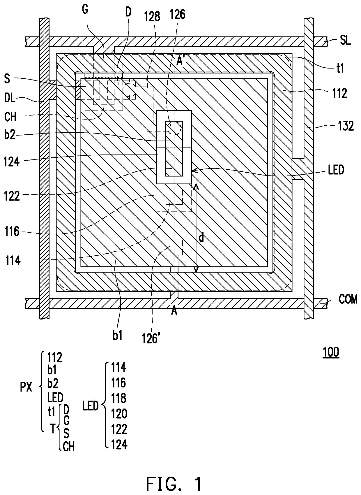
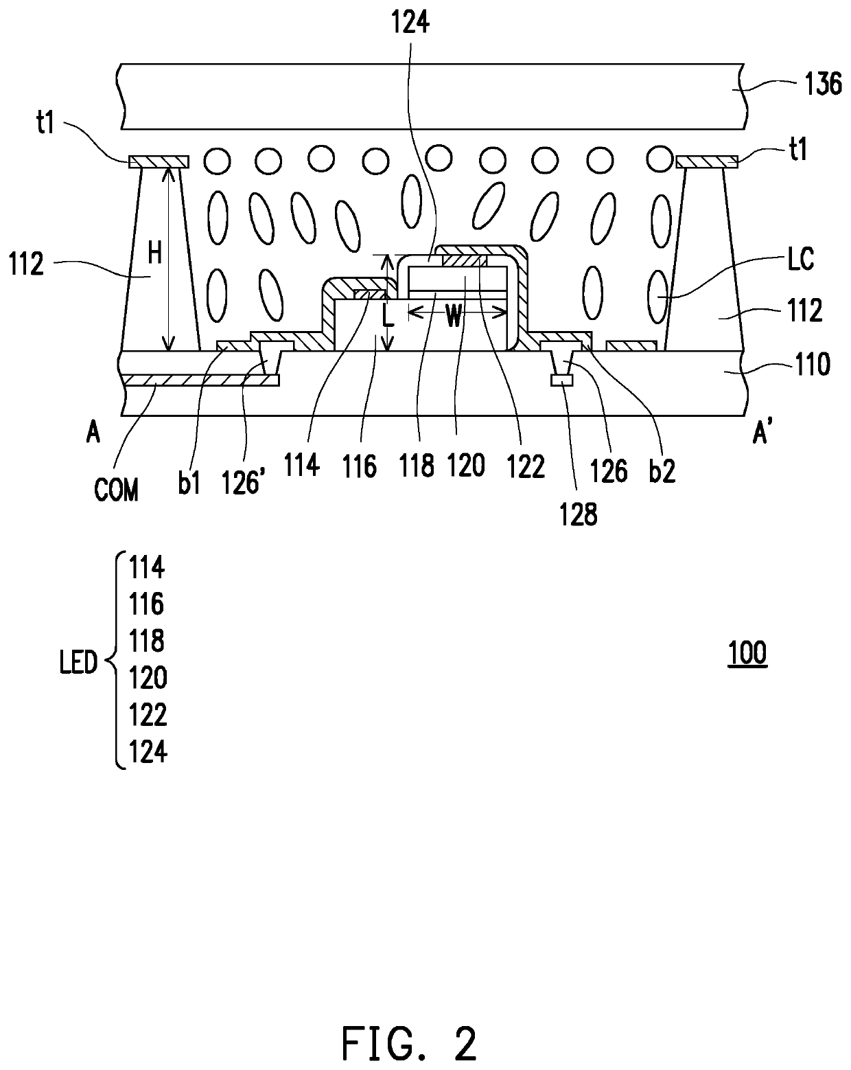
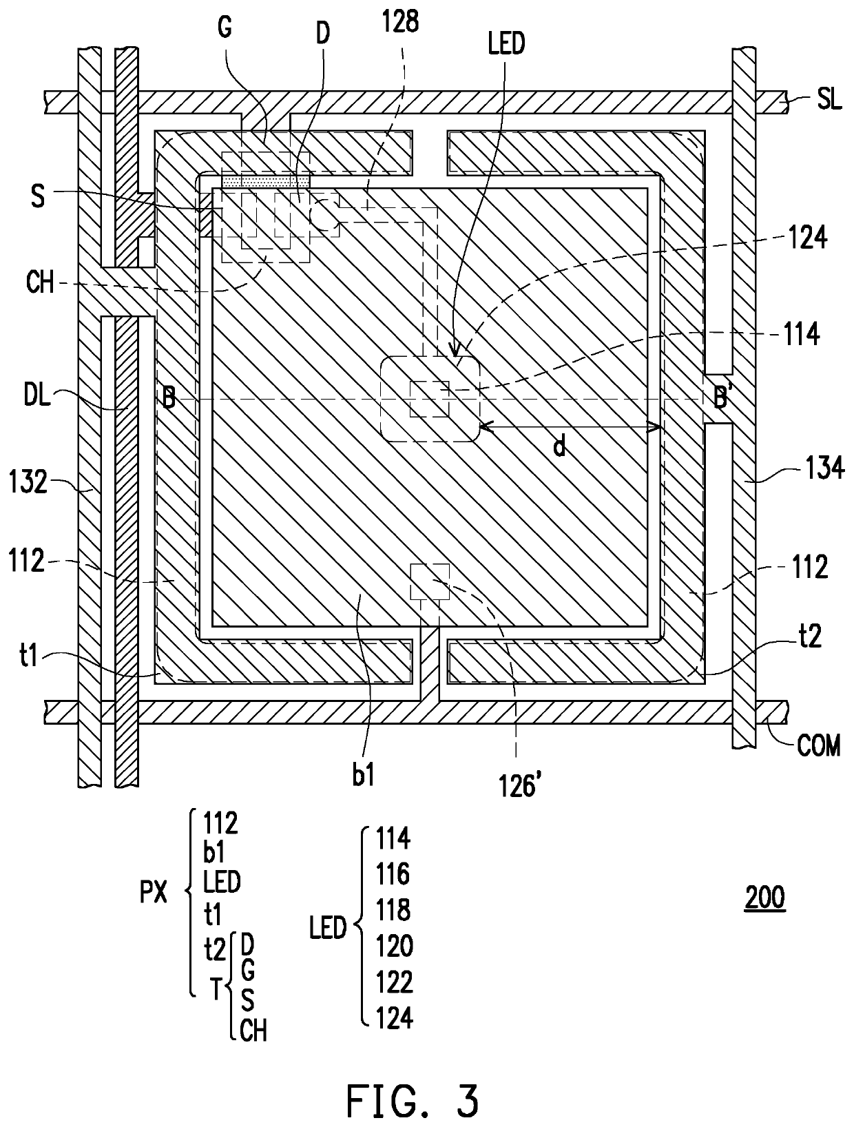
[0017]The present invention will be described more fully hereinafter with reference to the accompanying drawings, in which exemplary embodiments of the invention are shown. As those skilled in the art would realize, the described embodiments may be modified in various different ways, all without departing from the spirit or scope of the present invention.

[0018]Unless otherwise defined, all terms (including technical and scientific terms) used herein have the same meaning as commonly understood by one of ordinary skill in the art to which this invention belongs. It will be further understood that terms such as those defined in commonly used dictionaries should be interpreted as having a meaning that is consistent with their meaning in the context of the related art and the present invention and will not be interpreted as idealized or excessive. The formal meaning, unless explicitly defined in this article.

[0019]Exemplary embodiments are described herein with reference to cross-sectio...


PUM

PropertyMeasurementUnit
widthaaaaaaaaaa
widthaaaaaaaaaa
distanceaaaaaaaaaa

Abstract

A pixel array substrate and a driving method of a pixel array substrate are provided. The pixel array substrate includes a substrate, at least one pixel structure located on the substrate and a liquid crystal layer. The at least one pixel structure includes a micro light emitting diode (μLED), a supporting wall, a first bottom electrode located between the supporting wall and the μLED, and a first top electrode disposed on the supporting wall and separated from the first bottom electrode. The μLED includes a first electrode, a first semiconductor layer electrically connected to the first electrode, a second semiconductor layer, a light-emitting layer located between the first semiconductor layer and the second semiconductor layer, and a second electrode electrically connected to the second semiconductor layer. The liquid crystal layer is disposed on the first bottom electrode and located between the supporting wall and the μLED.

Description

CROSS-REFERENCE TO RELATED APPLICATION[0001]This application claims the priority benefit of Taiwan application serial no. 107115997, filed on May 10, 2018. The entirety of the above-mentioned patent application is hereby incorporated by reference herein and made a part of this specification.BACKGROUND1. Field of the Invention[0002]This disclosure is related to a substrate and a driving method of the substrate, especially related to a pixel array substrate and a driving method of the pixel array substrate.2. Description of Related Art[0003]A light emitting diode (LED) is a light emitting device, which is suitable for constructing a light emitting diode display panel because of its low power consumption, high brightness, high resolution, and high color saturation and the like. The micro light-emitting diodes (μLED) not only inherit the characteristics of the LEDs, but also reduce the volume of the pixel structure using the μLEDs to 1% of the volume of the pixel structure using the LED...

Claims


Application Information

Patent Timeline
Patent Type & Authority Applications(United States)
IPC IPC(8): H01L27/12G02F1/1362H01L27/15G09G3/36
CPCH01L27/156G02F1/1362G09G3/3648H01L27/124G09G3/32G02F1/133377G02F1/133603G02F1/134309G09G2300/0426G09G2300/046G09G2320/028G02F1/13793H01L25/0753H01L27/1244H01L33/44
Inventor YU, FANG-CHENGCHEN, CHEN-CHANGTSAO, TZU-YILIU, PIN-MIAOTSAI, CHENG-YEH
Owner AU OPTRONICS CORP
Why Eureka
Try Eureka