

Method for manufacturing transparent light emitting device by using UV imprinting technology and transparent light emitting device manufactured thereby
- Summary
- Abstract
- Description
- Claims
- Application Information
AI Technical Summary
Benefits of technology
Problems solved by technology
Method used
Image

Examples
Embodiment Construction
Technical Problem
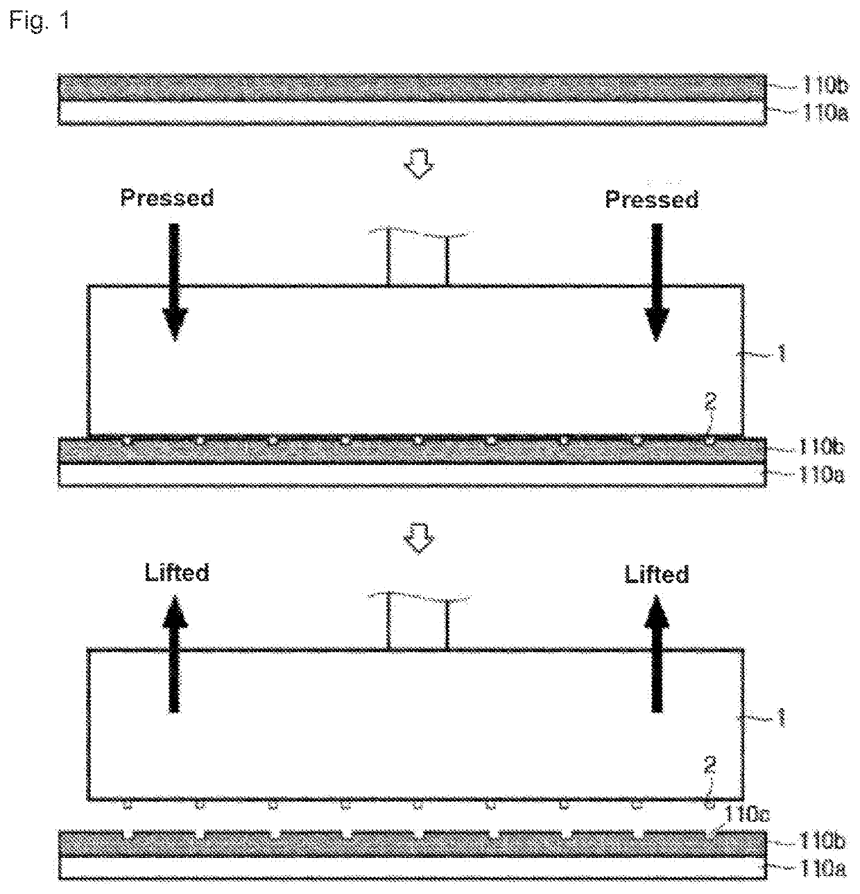
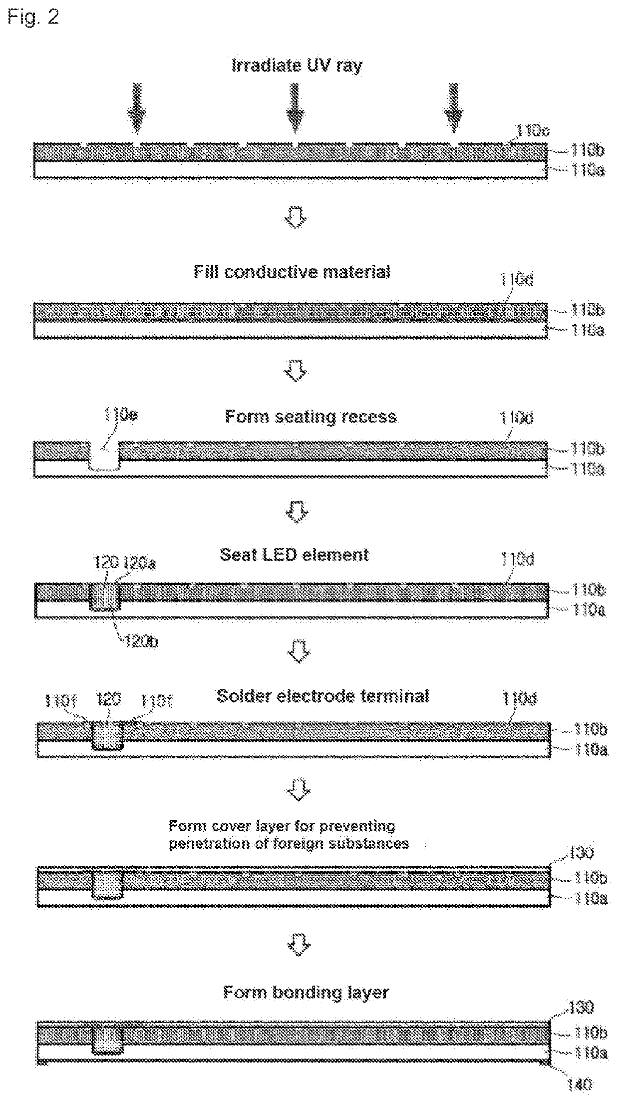
[0007]The present invention provides a method for manufacturing a transparent light emitting device and a transparent light emitting device manufactured thereby, by which an electric circuit in a form of a metal mesh can be formed by promptly imprinting an integral circuit pattern through a UV imprinting technology and filling a conductive material in the circuit pattern. In particular, the present invention provides a method for manufacturing a transparent light emitting device and a transparent light emitting device manufactured thereby, by which the number of manufacturing processes of the high-resolution transparent light emitting device of a large area can be minimized and productivity can be maximized by promptly imprinting an integral circuit pattern by using a mold.
Technical Solution
[0008]A method for manufacturing a transparent light emitting device using a UV imprinting technology according to an embodiment of the present invention includes: forming a subs...
PUM
 Abstract
Description
Claims
Application Information