Wafer support table
- Summary
- Abstract
- Description
- Claims
- Application Information
AI Technical Summary
Benefits of technology
Problems solved by technology
Method used
Image

Examples
Embodiment Construction
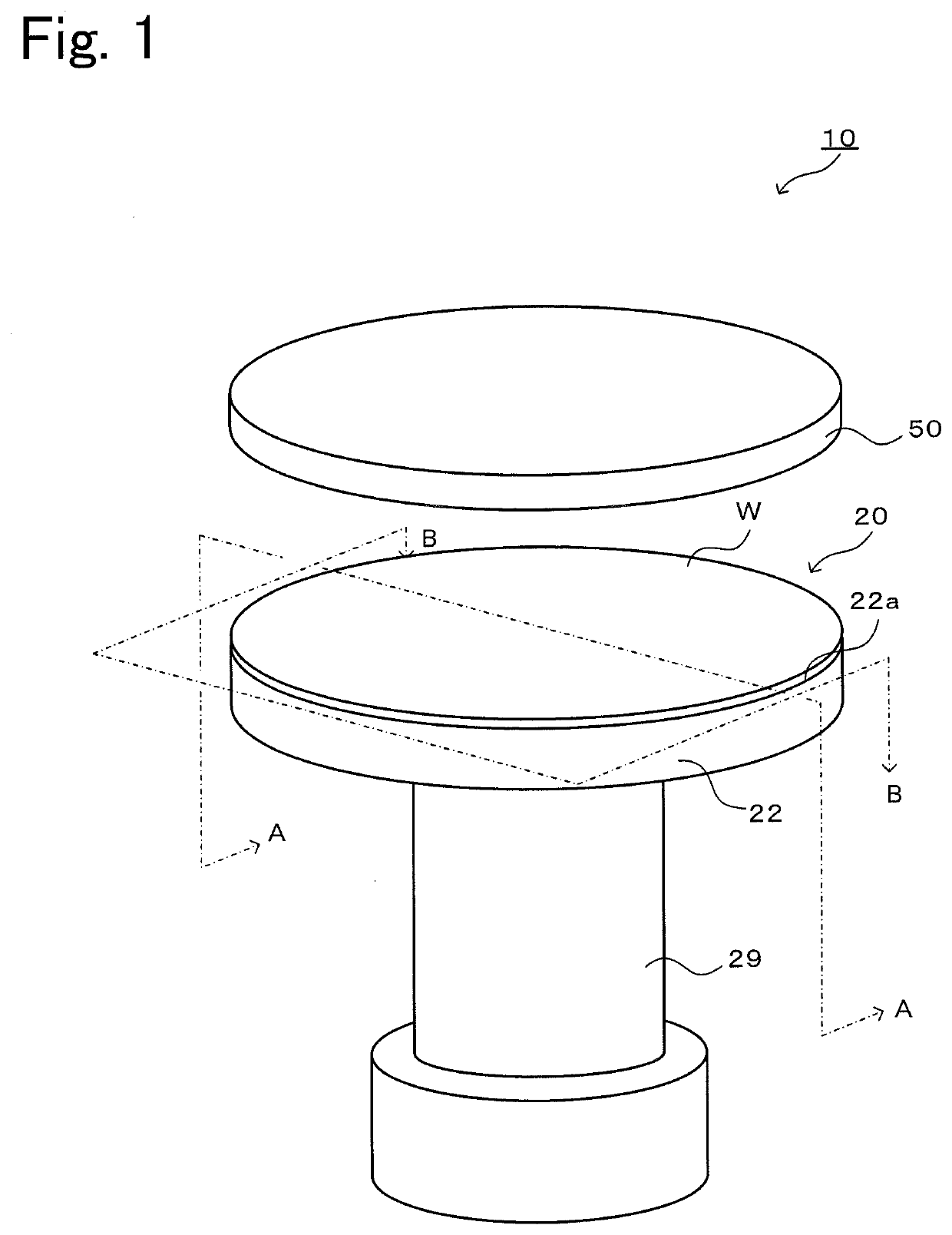
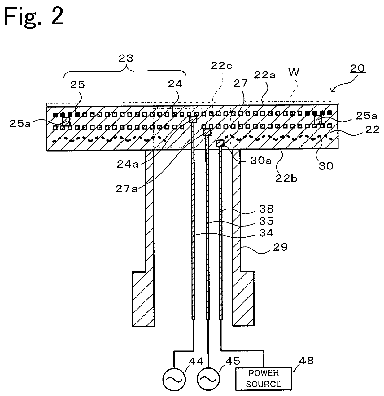
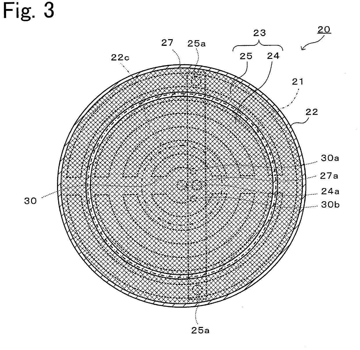
[0028]A preferred embodiment of the present invention is described below with reference to the drawings. FIG. 1 is a perspective view of a plasma generating device 10, FIG. 2 is a cross-sectional view taken along line A-A in FIG. 1, FIG. 3 is a cross-sectional view taken along line B-B in FIG. 1, and FIG. 4 is a perspective view illustrating a way in which an RF electrode 23, a jumper 27, and a heater electrode 30 are disposed.
[0029]As illustrated in FIG. 1, the plasma generating device 10 includes a wafer support table 20 and an upper electrode 50.
[0030]The wafer support table 20 is used to support and heat a wafer W on which CVD, etching, or the like is performed by using plasma and is attached inside a chamber for a semiconductor process (not illustrated). This wafer support table 20 includes a ceramic substrate 22 and a hollow ceramic shaft 29.
[0031]As illustrated in FIG. 2, the ceramic substrate 22 is a circular-plate-shaped member made of ceramic (e.g., alumina or aluminum nit...
PUM
 Abstract
Description
Claims
Application Information
 - Generate Ideas
- Intellectual Property
- Life Sciences
- Materials
- Tech Scout
- Unparalleled Data Quality
- Higher Quality Content
- 60% Fewer Hallucinations
Browse by: Latest US Patents, China's latest patents, Technical Efficacy Thesaurus, Application Domain, Technology Topic, Popular Technical Reports.
© 2025 PatSnap. All rights reserved.Legal|Privacy policy|Modern Slavery Act Transparency Statement|Sitemap|About US| Contact US: help@patsnap.com