Organic Device Having Protective Film and Method of Manufacturing the Same

a protective film and organic technology, applied in the field of organic devices having protective films, can solve the problems of shortening the life of increasing process time and manufacturing costs, and limited materials and shapes which may be applied to manufacture the organic light emitting device, so as to reduce the process time, reduce the deformation of the organic device, and minimize physical and chemical stress

Active Publication Date: 2019-11-21
KOREA ADVANCED INST OF SCI & TECH
View PDF25 Cites 0 Cited by
  • Summary
  • Abstract
  • Description
  • Claims
  • Application Information

AI Technical Summary

Benefits of technology

[0013]Since the organic device having the protective film according to the present invention may be attached to other materials through the bonding layer, it is not necessary to apply heat in order to attach the organic device to other materials, and as a result, it is possible to attach the organic device to various materials having various shapes regardless of types and shapes of materials.
[0014]According to the organic device having the protective film according to the present invention, since the protective film is formed as the substrate having the bonding layer is attached to the organic device, no heat is applied to the organic device during the process of forming the protective film, and as a result, it is possible to minimize deformation of the organic device by minimizing physical and chemical stress to be applied to the organic device.
[0015]According to the organic device having the protective film according to the present invention, the two protective film layers for protecting the organic device are manufactured through the same process, and as a result, it is possible to innovatively reduce the process time required to manufacture the organic device having the protective film in comparison with the process in the related art.
[0016]The substrate having upper / lower protective films has a sandwich structure and defines a structure for protecting the organic device, such that a neutral axis is naturally formed on the organic device, and as a result, it is possible to minimize bending stress to be applied to the organic device.

Problems solved by technology

Therefore, a material and a shape, which may be applied to manufacture the organic light emitting device, are very limited.
Because of these problems, there is a problem in that the process time and the manufacturing costs are increased to manufacture the organic light emitting devices having various materials or various shapes.
In addition, because the organic light emitting device is generally vulnerable to moisture and oxygen, it is necessary to form a multilayer encapsulation film on a lower surface of the organic light emitting device as well as an upper surface of the organic light emitting device.
Therefore, if the multilayer encapsulation film is formed only on the upper surface of the organic light emitting device and the organic light emitting device is formed on a material having high moisture permeability, there is a problem in that the moisture, which permeates into the material, may shorten a lifespan of the organic light emitting device.
Therefore, in the related art, there is a problem in that a large amount of manufacturing process time is generally required because a process of forming a multilayer encapsulation film on a substrate, forming an organic light emitting device, and then forming a multilayer encapsulation film on the organic light emitting device again needs to be performed to form the multilayer encapsulation film even on the lower surface of the organic light emitting device.
Further, there is a problem in that the organic light emitting device having a protective film manufactured by the above-mentioned processes has a limitation in terms of durability and reliability associated with mechanical stress such as bending and warping because a neutral axis is positioned to be closer to the substrate than the organic light emitting device.
Therefore, there is a problem in that the organic light emitting device has a low ability of withstanding mechanical stress such as bending and scratches that may occur during a process of washing the material to which the organic light emitting device manufactured by the general process is attached after attaching the organic light emitting device to the material.
That is, as described above, there is a problem in that there is a great limitation in applying the organic light emitting device in the related art to application fields associated with wearable, healthcare, and illumination in addition to the application field associated with the flat panel display.

Method used


Image

  • Organic Device Having Protective Film and Method of Manufacturing the Same
  • Organic Device Having Protective Film and Method of Manufacturing the Same
  • Organic Device Having Protective Film and Method of Manufacturing the Same

Examples


Embodiment Construction

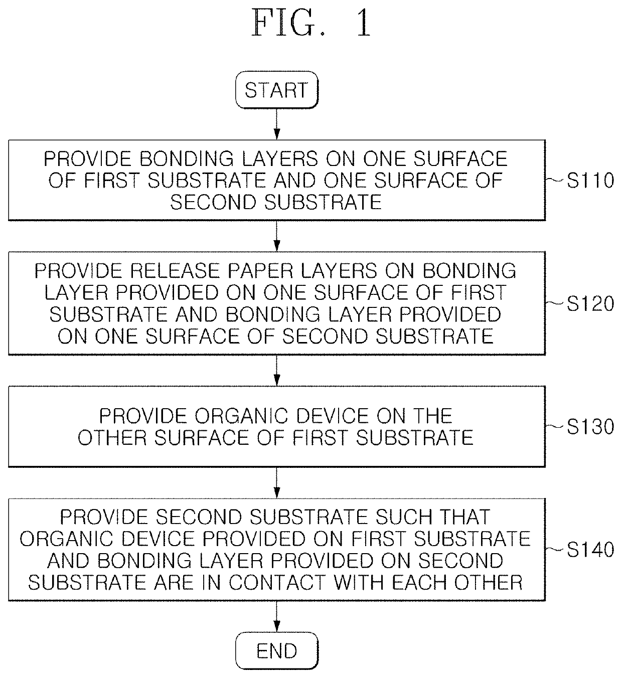
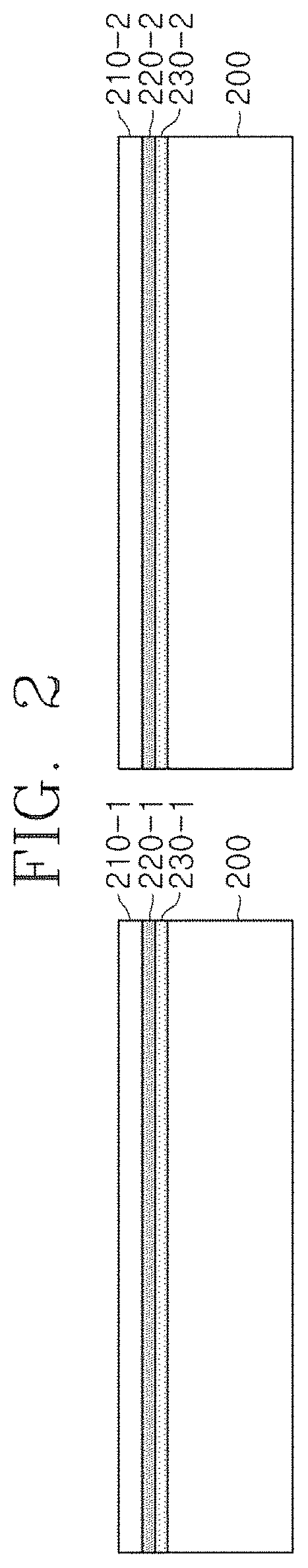
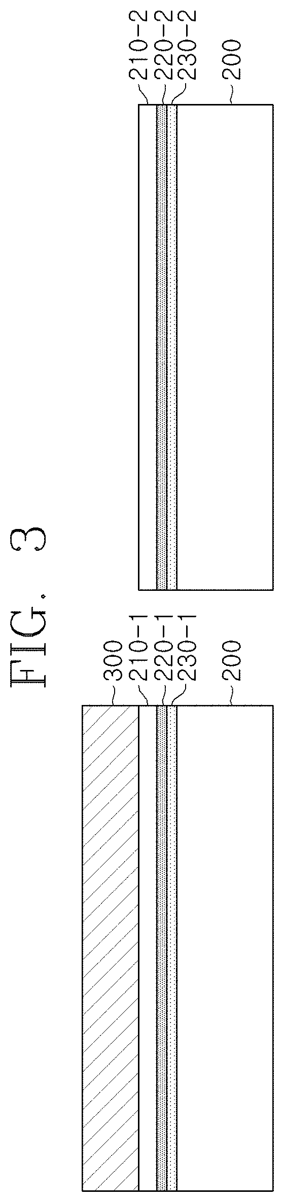
[0030]Hereinafter, exemplary embodiments disclosed in the present specification will be described in detail with reference to the accompanying drawings. The same or similar constituent elements are assigned with the same reference numerals regardless of reference numerals, and the repetitive description thereof will be omitted. In the description of the exemplary embodiments disclosed in the present specification, the specific descriptions of publicly known related technologies will be omitted when it is determined that the specific descriptions may obscure the subject matter of the exemplary embodiments disclosed in the present specification. In addition, it should be interpreted that the accompanying drawings are provided only to allow those skilled in the art to easily understand the exemplary embodiments disclosed in the present specification, and the technical spirit disclosed in the present specification is limited by the accompanying drawings, and includes all alterations, eq...


PUM

PropertyMeasurementUnit
thicknessaaaaaaaaaa
thicknessaaaaaaaaaa
stress degreeaaaaaaaaaa

Abstract

The present invention provides a method of manufacturing an organic device having a protective film, the method including: providing bonding layers (adhesives) on one surface of a first substrate and one surface of a second substrate; providing an organic device on the other surface of the first substrate; and providing the second substrate on the organic device such that the bonding layer (adhesive) provided on the second substrate is in contact with the organic device. Since the organic device having the protective film according to the present invention may be attached to other materials through the bonding layer (adhesive), it is not necessary to apply heat in order to attach the organic device to other materials, and as a result, it is possible to attach the organic device to various materials having various shapes regardless of types and shapes of materials. Further, according to the organic device having the protective film according to the present invention, since the protective film is formed as the substrate having the bonding layer (adhesive) 220 is attached to the organic device 300, no heat is applied to the organic device 300 during the process of forming the protective film, and as a result, it is possible to minimize deformation of the organic device 300 by minimizing physical and chemical stress to be applied to the organic device 300. According to the organic device having the protective film according to the present invention, the two protective film layers for protecting the organic device are manufactured through the same process, and as a result, it is possible to innovatively reduce the process time required to manufacture the organic device having the protective film in comparison with the process in the related art.

Description

CROSS-REFERENCE TO RELATED APPLICATIONS[0001]This application claims priority to Korean Patent Application No. 10-2018-0057742 filed on May 21, 2018 and Korean Patent Application No. 10-2019-0007536 filed on Jan. 21, 2019, the disclosures of which are hereby incorporated by reference in their entirety.BACKGROUND OF THE INVENTIONField of the Invention[0002]The present invention relates to an organic device having a protective film and a method of manufacturing the same, and more particularly, to an organic device having a protective film which is manufactured by a method of providing two substrates each having one surface on which a bonding layer is formed and the other surface on which a encapsulation film layer is formed, and forming the organic device sandwiched between the provided two substrates, and a method of manufacturing the same.Description of the Related Art[0003]Recently, a display field for visually expressing electrical information signals has been rapidly developed as...

Claims


Application Information

Patent Timeline
Patent Type & Authority Applications(United States)
IPC IPC(8): H01L51/52H01L51/00H01L51/56
CPCH01L2251/303H01L51/5253H01L2251/558H01L51/0028H01L51/56H10K50/841H10K50/8426H10K50/844H10K71/00H10K71/441H10K2102/00H10K2102/351
Inventor CHOI, KYUNG CHEOLJEON, YONG MIN
Owner KOREA ADVANCED INST OF SCI & TECH
Why Eureka
Try Eureka