Self-aware and correcting heterogenous platform incorporating integrated semiconductor processing modules and method for using same
Pending Publication Date: 2020-01-02
TOKYO ELECTRON LTD
View PDF2 Cites 6 Cited by
Summary
Abstract
Description
Claims
Application Information
AI Technical Summary
This helps you quickly interpret patents by identifying the three key elements:
Problems solved by technology
Method used
Benefits of technology
[0014]This disclosure relates to a high volume manufacturing platform which incorporates metrology instruments integrated to measure workpieces before and/or after being treated in the platform's processing chambers. Transfer chambers connected to the process chambers are integrated with the metrology sensors to enable measurements being done within the platform, and not a stand-alone metrology tool. In this instance, maintaining workpieces within the platform's controlled environment reduces the potential for added particles by reducing workpiece movement and minimizing the exposure of different environments to the workpiece. Broadly, the measurements may implemented with the platform in a variety of ways an
Problems solved by technology
For example, as smaller circuits such as transistors are manufactured, the critical dimension (CD) or resolution of patterned features is becoming more challenging to produce.
However, it has become extremely difficult to produce scaled devices at reasonably low cost.
However, such resources do not contribute to throughput and production, and as a result, are purely costs for the fabricators.
Furthermore, when a process goes out of specification, and the features of the substrate are not properly fabricated, it may be necessary to remove the substrate from production.
This also introduces uncertainty in any measurements where the substrate has to be brought out of a vacuum or other controlled environment and then introduced into the metrology kiosk.
Accordingly, fabricators may not be certain that they are measuring the parameters that they believe they are measuring.
As such, with smaller feature sizes in three-dimensional devices/architectures, current monitoring technologies and measurement and metrology processes are inadequate.
As a result, there can often be a lag in time between a particular process going out of specification and the recognition of that fact.
This furth
Method used
Image
Click on the blue label to locate the original text in one second.
Reading with bidirectional positioning of images and text.
Examples
examples
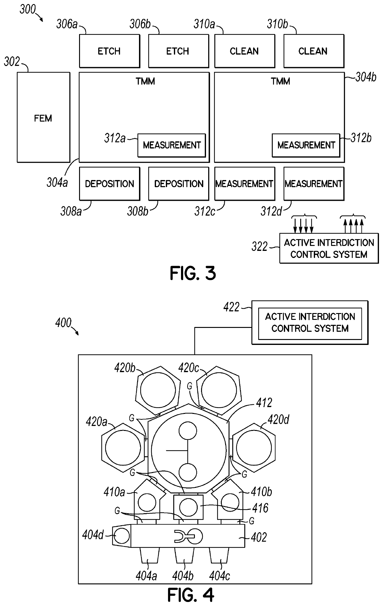
[0247]FIGS. 13A-13E set forth one example of active interdiction in area selective deposition for removal of undesired nuclei on a self-aligned mono layer through active interdiction.
[0248]Referring now to FIGS. 13A-13E, according to one exemplary embodiment, the manufacturing platform with an active interdiction control system may be configured to perform and monitor a method of area selective deposition on a substrate and to gather measurement data and other data. In this embodiment, the substrate 1300 contains a base layer 1302, an exposed surface of a first material layer 1304 and an exposed surface of a second material layer 1306. In one example, the substrate includes a dielectric layer 1304 and a metal layer 1306. For example, the metal layer 1306 can contain Cu, Al, T a, Ti, W, Ru, Co, Ni, or Mo. The dielectric layer 1304 can, for example, contain SiO2, a low-k dielectric material, or a high-k dielectric material. Low-k dielectric materials have a nominal dielectric constant...
PUM
Abstract
This disclosure relates to a high volume manufacturing system for processing and measuring workpieces in a semiconductor processing sequence without leaving the system's controlled environment (e.g., sub-atmospheric pressure). The systems process chambers are connected to each other via transfer chambers used to move the workpieces, in the controlled environment, between the process chambers. Further, the pass-through chambers may be disposed between the transfer chambers or between the transfer chamber and the process chamber. The pass-through chambers may include a measurement region to measure workpiece attributes when the workpiece is moved through or placed in the pass-through chamber. The transfer chambers may also have separate measurement regions within their internal space to measure other attributes of the workpiece.
Description
CROSS-REFERENCE TO RELATED APPLICATIONS[0001]The present application claims the benefit of U.S. Provisional Application No. 62 / 645,685, filed on Mar. 20, 2018, entitled “Substrate Processing Tool with Integrated Metrology and Method of Using,” U.S. Provisional Application No. 62 / 787,607, filed on Jan. 2, 2019, entitled “Self-Aware and Correcting Heterogeneous Platform incorporating Integrated Semiconductor Processing Modules and Method for using same,” U.S. Provisional Application No. 62 / 787,608, filed on Jan. 2, 2019, entitled “Self-Aware and Correcting Heterogeneous Platform incorporating Integrated Semiconductor Processing Modules and Method for using same,” and U.S. Provisional Application No. 62 / 788,195, filed on Jan. 4, 2019, entitled “Substrate Processing Tool with Integrated Metrology and Method of using,” and U.S. Provisional Application No. 62 / 787,874, filed on Jan. 3, 2019, entitled “Self-Aware and Correcting Heterogenous Platform Incorporating Integrated Semiconductor Pr...
Claims
Application Information
Patent Timeline
Application Date:The date an application was filed.
Publication Date:The date a patent or application was officially published.
First Publication Date:The earliest publication date of a patent with the same application number.
Issue Date:Publication date of the patent grant document.
PCT Entry Date:The Entry date of PCT National Phase.
Estimated Expiry Date:The statutory expiry date of a patent right according to the Patent Law, and it is the longest term of protection that the patent right can achieve without the termination of the patent right due to other reasons(Term extension factor has been taken into account ).
Invalid Date:Actual expiry date is based on effective date or publication date of legal transaction data of invalid patent.