Testing method for semiconductor memory

a technology of semiconductor memory and test method, which is applied in the direction of information storage, static storage, digital storage, etc., can solve the problems of deemed defective semiconductor memory, and achieve the effect of small variation in performan

Active Publication Date: 2020-01-23
LAPIS SEMICON CO LTD
View PDF0 Cites 3 Cited by
  • Summary
  • Abstract
  • Description
  • Claims
  • Application Information

AI Technical Summary

Benefits of technology

[0004]The present invention was made in view of this point, and an object thereof is to provide a testing method for semiconductor memory that makes it possible to manufacture semiconductor memory while suppressing the variations in performance.
[0009]In accordance with the testing method for semiconductor memory of the present invention, it is possible to manufacture semiconductor memory having a smaller degree of variations in performance.

Problems solved by technology

If the number of defective cells exceeds the number of redundant cells, that semiconductor memory is deemed defective.

Method used


Image

  • Testing method for semiconductor memory
  • Testing method for semiconductor memory
  • Testing method for semiconductor memory

Examples


embodiment 1

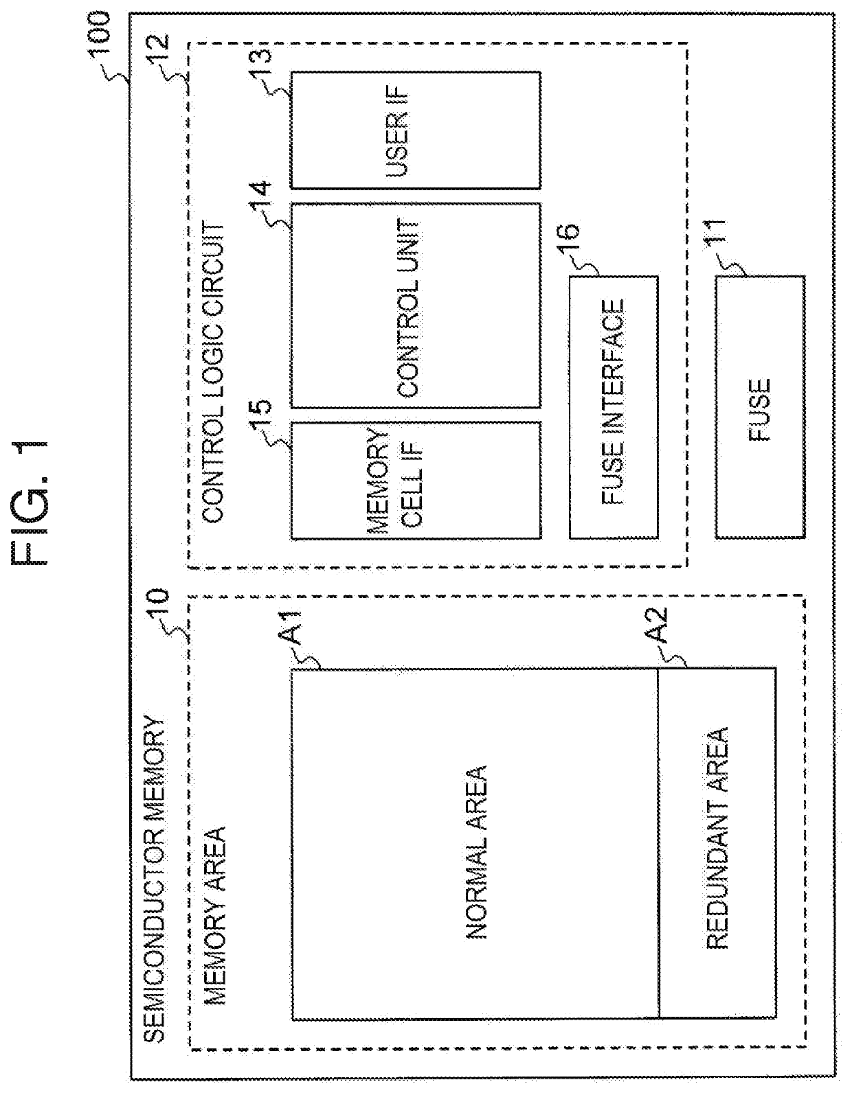
[0017]FIG. 1 is a block diagram illustrating the configuration of semiconductor memory 100 of a first embodiment. The semiconductor memory 100 is constituted of a DRAM (dynamic random access memory), for example. The semiconductor memory 100 includes a memory area 10, a fuse 11, and a control logic circuit 12.

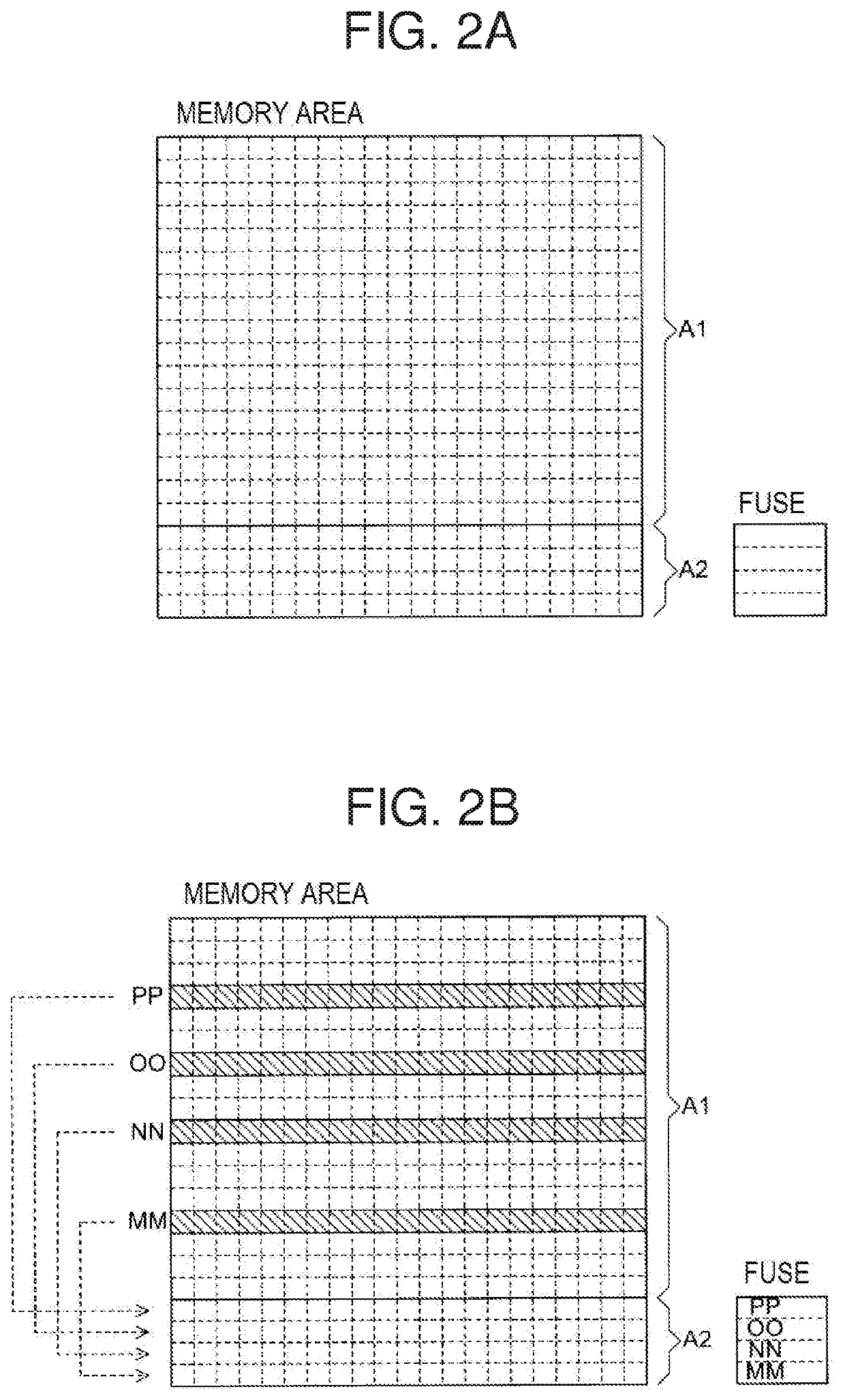
[0018]The memory area 10 includes a normal area A1 and a redundant area A2. The normal area A1 is a memory area made up of memory cells to be accessed in a regular memory access process. The redundant area A2 is a memory area including redundant blocks that replace blocks in the normal area A1 which include more defective cells than a prescribed number (referred to throughout the specification as defective blocks).

[0019]The fuse 11 stores the address of each defective block as a “redundant address” in association with the address of a redundant block to be replaced with. The fuse 11 is constituted of a plurality of fuse elements, and stores the information of redundant address ...

embodiment 2

[0043]Next, another embodiment of the present invention will be explained. The testing method of this embodiment differs from the testing method of the first embodiment in that a defective block to be replaced with a redundant block is selected by turning off the semiconductor memory 100 and then turning it back on, instead of repeating the test to determine defective cells.

[0044]One of the characteristics of DRAM is that when the power is turned off and then turned back on, electrical charges are accumulated in some of the memory cells with an increase in cell plate potential, which is the internal power source. Those charges vary depending on the capacity of each memory cell, and can therefore be read out as random data for each chip before actual data is written in DRAM.

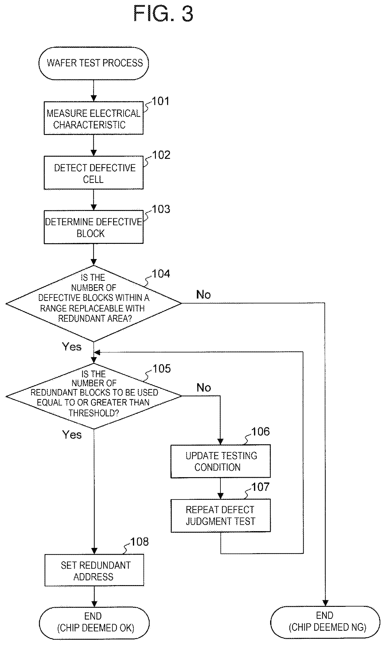
[0045]The test process of this embodiment will be explained with reference to the flowchart of FIG. 4.

[0046]First, each of the plurality of chips formed on a wafer undergoes the defect judgment test to detect defe...


PUM


Abstract

A testing method for a semiconductor memory includes determining which memory blocks are defective based on the number of defective cells in the block. The method includes determining whether the number of defective blocks exceeds a first threshold value and judging the semiconductor memory to be defective if the number of defective blocks is equal to or greater than the first threshold value. The method also includes comparing the number of defective blocks with a second threshold value equal to or less than the first threshold value and repeating the process of measuring and judging of the memory cells and memory blocks until the number of defective blocks is at least equal to the second threshold value, and then managing access to the defective blocks in a different manner from accesses to other blocks.

Description

BACKGROUND OF THE INVENTIONTechnical Field[0001]The present invention relates to a testing method for semiconductor memory.Background Arts[0002]In the manufacturing process of semiconductor memory such as dynamic random access memory (DRAM), a test to determine the quality of semiconductor memory is conducted in a wafer test process, which is performed on a wafer on which the semiconductor memory is formed (see Japanese Patent Application Laid-open Publication No. 2008-108395, for example). In this test, memory cells that do not satisfy prescribed operation conditions are deemed defective cells. A semiconductor memory has a redundant area in addition to a normal memory area, and cells in the redundant area (redundant cells) replace the memory cells deemed defective in the test. That is, when the address of a defective cell is to be accessed, the address of the redundant cell, instead of the defective cell, is accessed. If the number of defective cells exceeds the number of redundant...

Claims


Application Information

Patent Timeline
Patent Type & Authority Applications(United States)
IPC IPC(8): G11C29/00G11C29/50G11C11/4096
CPCG11C29/50G11C11/4096G11C2029/5004G11C29/76G11C29/785G11C29/02G11C29/50004G11C29/56G11C29/838G11C29/006G11C29/44G11C7/04
Inventor OKADA, TOSHIHARU
Owner LAPIS SEMICON CO LTD
Why Eureka
Try Eureka