

Inductor component
a technology of components and components, applied in the direction of transformers/inductance coils/windings/connections, conductive pattern formation, inductance, etc., can solve the problem of insufficient improvement of q value of conventional inductor components, and achieve sufficient mechanical strength and reduce the refractive index of crystals
- Summary
- Abstract
- Description
- Claims
- Application Information
AI Technical Summary
Benefits of technology
Problems solved by technology
Method used
Image

Examples
first embodiment
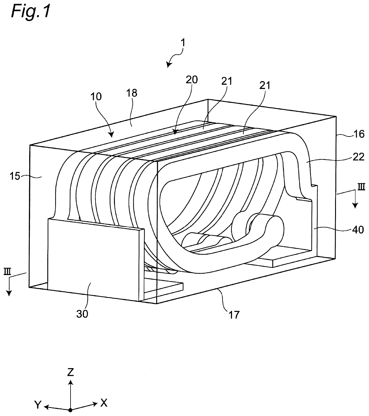
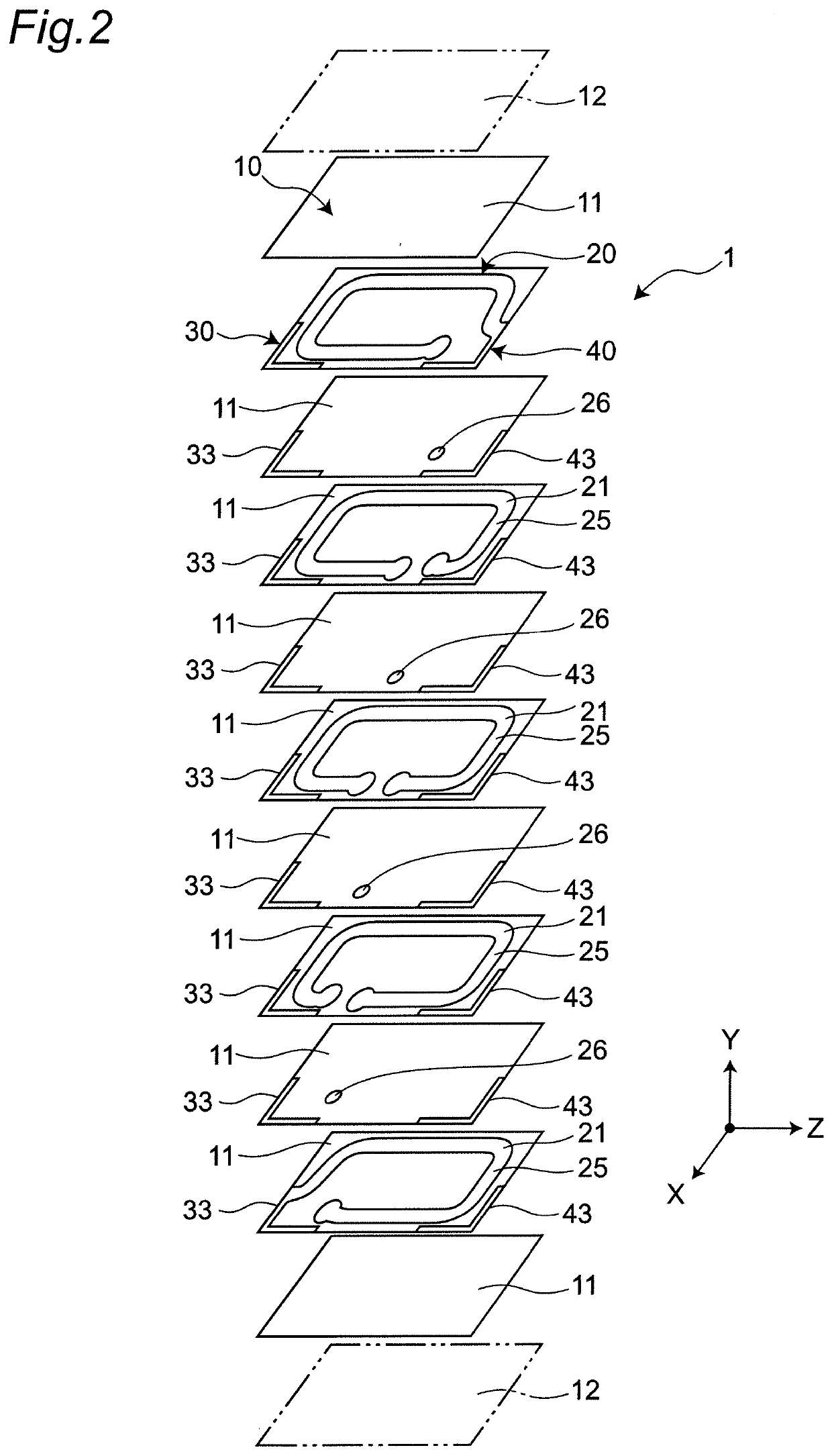
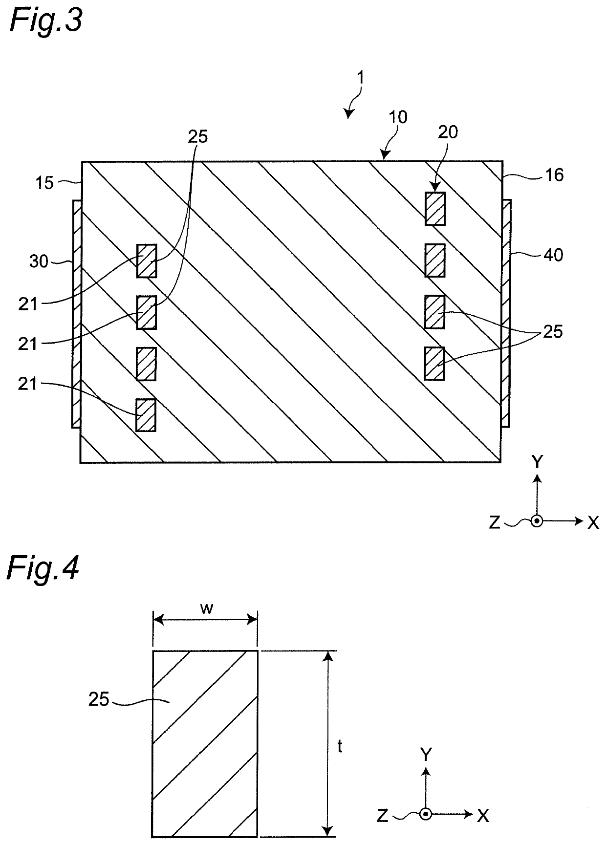
[0052]FIG. 1 is a transparent perspective view showing a first embodiment of an inductor component. FIG. 2 is an exploded perspective view of the inductor component. FIG. 3 is a cross-sectional view of the inductor component. As shown in FIGS. 1, 2, and 3, an inductor component 1 has an element body 10, a helical coil 20 disposed inside the element body 10, and a first external electrode 30 and a second external electrode 40 disposed on the element body 10 and electrically connected to the coil 20. In FIG. 1, the element body 10 is transparently drawn so that a structure can easily be understood. FIG. 3 shows a cross section taken along a line III-III of FIG. 1.
[0053]The inductor component 1 is electrically connected via the first and second external electrodes 30, 40 to a wiring of a circuit board not shown. The inductor component 1 is used as an impedance matching coil (matching coil) of a high-frequency circuit, for example, and is used for an electronic device such as a personal...
second embodiment
[0081]FIG. 5 is a cross-sectional view showing a second embodiment of the inductor component. The second embodiment is different from the first embodiment in configuration of coil wirings. This different configuration will hereinafter be described.
[0082]Although the coil wiring 21 of the first embodiment is made up of a single layer as shown in FIGS. 3 and 4, a coil wiring 21A of the second embodiment is made up of three coil conductor layers 25a, 25b, 25c laminated in surface contact with each other as shown in FIG. 6. The coil wiring 21A may be made up of two or four or more coil conductor layers.
[0083]Specifically, the coil wiring 21A is formed as multiple stages. For example, a first groove is formed in a first insulating layer 11a, and the first coil conductor layer 25a is embedded in the first groove. Subsequently, a second insulating layer 11b is formed on the first insulating layer 11a, a second groove is formed in the second insulating layer 11b, and the second coil conduct...
third embodiment
[0097]FIG. 9 is a cross-sectional view showing a third embodiment of the inductor component. The third embodiment is different from the second embodiment in configuration of the coil wiring. This different configuration will hereinafter be described.
[0098]Although the coil wiring 21A of the second embodiment is made up of the coil conductor layers 25a, 25b, 25c having a rectangular cross section as shown in FIG. 6, a coil wiring 21B of the third embodiment is made up of the coil conductor layers 25a, 25b, 25c having a T-shaped cross section, and the cross section of the coil wiring 21B has a stacked shape of T.
[0099]In this case, although the cross section of the coil wiring 21B is T-shaped, the aspect ratio of the coil wiring 21B can be calculated from the cross-sectional area of the coil wiring 21B and the maximum thickness of the coil wiring 21B in the axial direction. Specifically, the aspect ratio is (thickness t of the coil wiring 21B) / (wiring width W of the coil wiring 21B), ...
PUM
| Property | Measurement | Unit |
|---|---|---|
| refractive index | aaaaa | aaaaa |
| aspect ratio | aaaaa | aaaaa |
| aspect ratio | aaaaa | aaaaa |
Abstract
Description
Claims
Application Information