Wafer processing method

a processing method and wafer technology, applied in the field of wafer processing method, can solve the problems of device chips coming into abnormal contact with the cutting blade being rotated, device chips degrading in quality, and affecting so as to achieve the effect of degrading the quality of the device chip

Active Publication Date: 2020-01-30
DISCO CORP
View PDF0 Cites 15 Cited by
  • Summary
  • Abstract
  • Description
  • Claims
  • Application Information

AI Technical Summary

Benefits of technology

[0004]As described above, the wafer is supported through the dicing tape by the annular frame in dividing the wafer into individual device chips, so that it becomes possible to transfer the wafer to a subsequent step in the condition of keeping the form of the whole wafer after being diced. However, when the wafer is subjected to dicing along the division lines by use of a cutting blade, a chipping occurs on the back surface side of the wafer where the wafer is attached to the dicing tape, thereby causing degradation in quality of a device chip.

Problems solved by technology

However, when the wafer is subjected to dicing along the division lines by use of a cutting blade, a chipping occurs on the back surface side of the wafer where the wafer is attached to the dicing tape, thereby causing degradation in quality of a device chip.
The above problem of degradation in quality of a device chip is attributable to a relatively soft adhesive layer which is formed on a front surface of the dicing tape.
Since such soft adhesive layer does not have adhesive force large enough to hold the wafer, the device chips move when the wafer is divided.
As a result, the device chips come into abnormal contact with the cutting blade being rotated.
This causes an abnormal contact between each device chip and the cutting blade being rotated, which is also considered to be a cause of a chipping of each device chip.
However, since the substrate has no adhesion by itself, it is necessary to unite the wafer and the substrate though a liquid resin, a wax, or an adhesive tape on which an adhesive agent or the like is coated.
In this case, when the dicing is finished and the substrate is separated from the back surface of the wafer, a liquid resin, a wax, or an adhesive agent or the like coated on an adhesive tape on which is coated is left on each device chip, newly causing another problem of degradation in quality of each device chip.

Method used


Image

  • Wafer processing method
  • Wafer processing method
  • Wafer processing method

Examples


Embodiment Construction

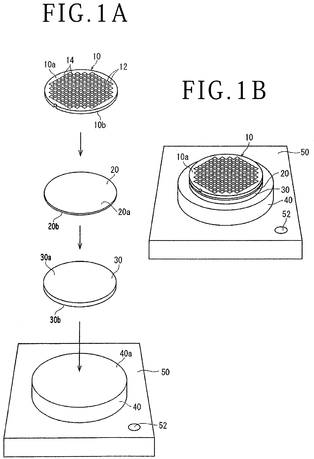
[0024]A preferred embodiment of a wafer processing method according to the present invention will be described in detail below with reference to the attached drawings. Upon carrying out the wafer processing method according to the present embodiment, first, as illustrated in FIG. 1A, a wafer 10 as a workpiece, a sheet 20, and a substrate 30 are prepared. The wafer 10 has a front surface 10a and a back surface 10b. The front surface 10a of the wafer 10 is partitioned by a plurality of division lines 14 in a grid pattern into individual separate regions where a plurality of devices 12 are individually formed. The sheet 20 has a front side 20a and a back side 20b. The sheet 20 is set to a size (diameter) substantially equal to that of the wafer 10 and is a thermoplastic polymer sheet such as a polyolefin sheet and a polyester sheet. In the present embodiment, a polyethylene (PE) sheet as an example of the polyolefin sheet is selected for the sheet 20. Also, the substrate 30 has a front...


PUM

PropertyMeasurementUnit
temperatureaaaaaaaaaa

Abstract

A wafer processing method includes: a wafer providing step of providing a wafer by placing a thermoplastic polymer sheet on an upper surface of a substrate on which the wafer is supported and positioning a back surface of the wafer on an upper surface of the polymer sheet; a sheet thermocompression bonding step of evacuating an enclosing environment in which the wafer is provided through the polymer sheet on the substrate, heating the polymer sheet, and pressing the wafer toward the polymer sheet to pressure-bond the wafer through the polymer sheet to the substrate; and a dividing step of positioning a cutting blade on the front surface of the wafer and cutting the wafer along the division lines to divide the wafer into individual device chips.

Description

BACKGROUND OF THE INVENTIONField of the Invention[0001]The present invention relates to a wafer processing method of dividing a wafer along a plurality of crossing division lines into individual device chips, the division lines being formed on a front surface side of the wafer to thereby define a plurality of separate regions where a plurality of devices are individually formed.Description of the Related Art[0002]A wafer has a plurality of devices such as integrated circuits (ICs) and large-scale integrations (LSIs) formed in separate regions defined by a plurality of crossing division lines on a front surface side of the wafer. After a back surface of the wafer is ground by using a grinding apparatus to reduce a thickness of the wafer to a predetermined thickness, the wafer is divided into individual device chips using a dicing apparatus. Accordingly, the device chips thus divided are used in electric equipment such as mobile phones and personal computers.[0003]In dividing a wafer ...

Claims


Application Information

Patent Timeline
Patent Type & Authority Applications(United States)
IPC IPC(8): H01L21/78H01L21/683C08J5/18
CPCC08J2325/06C08J2323/12H01L21/6836H01L21/78C08J5/18C08J2323/06C08J2367/02H01L2221/68327H01L2221/68386H01L21/67092H01L21/67132H01L21/67103H01L21/6838H01L21/67109H01L21/6835H01L2221/68381H01L21/76H01L21/185H01L21/324H01L21/67098H01L21/67248
Inventor HARADA, SHIGENORIOKAMURA, TAKASHIZHAO, JINYAN
Owner DISCO CORP
Why Eureka
Try Eureka