
Vertical transient voltage suppression device

a voltage suppression and transient technology, applied in semiconductor devices, diodes, electrical apparatuses, etc., can solve problems such as malfunctions of these electronics that could be reset or even damaged under electrostatic discharge events, and achieve low holding voltage, low clamping voltage, and enhanced electrostatic discharge performance

Active Publication Date: 2020-01-30
AMAZING MICROELECTRONICS
View PDF0 Cites 3 Cited by
  • Summary
  • Abstract
  • Description
  • Claims
  • Application Information

AI Technical Summary

Benefits of technology

The present invention provides a vertical transient voltage suppression device that helps to maintain a low holding voltage and a low clamping voltage, and enhance the electrostatic discharge (ESD) performance. This device achieves this by floating the base of a vertical bipolar junction transistor (BJT).

Problems solved by technology

Without suitable protection devices, the functions of these electronics could be reset or even damaged under electrostatic discharge (ESD) events.

Method used


Image

  • Vertical transient voltage suppression device
  • Vertical transient voltage suppression device
  • Vertical transient voltage suppression device

Examples


Embodiment Construction

[0028]Reference will now be made in detail to embodiments illustrated in the accompanying drawings. Wherever possible, the same reference numbers are used in the drawings and the description to refer to the same or like parts. In the drawings, the shape and thickness may be exaggerated for clarity and convenience. This description will be directed in particular to elements forming part of, or cooperating more directly with, methods and apparatus in accordance with the present disclosure. It is to be understood that elements not specifically shown or described may take various forms well known to those skilled in the art. Many alternatives and modifications will be apparent to those skilled in the art, once informed by the present disclosure.

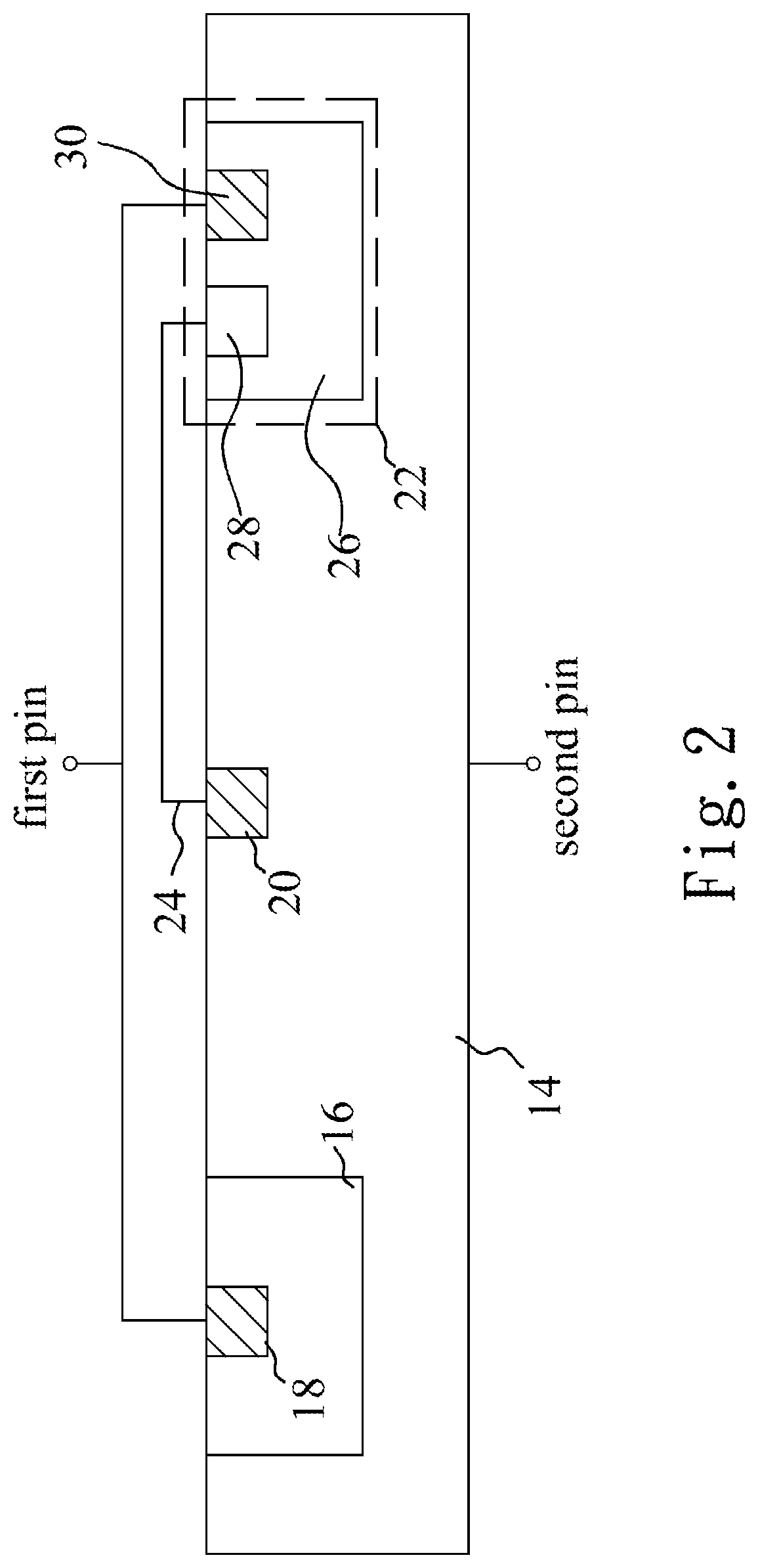
[0029]Refer to FIG. 2. The first embodiment of a vertical transient voltage suppression device of the present invention is introduced as follows. The vertical transient voltage suppression device comprises a semiconductor substrate 14 having a fi...


PUM

PropertyMeasurementUnit
conductivity typeaaaaaaaaaa
conductivityaaaaaaaaaa
sizesaaaaaaaaaa

Abstract

A vertical transient voltage suppression device includes a semiconductor substrate having a first conductivity type, a first doped well having a second conductivity type, a first heavily-doped area having the first conductivity type, a second heavily-doped area having the first conductivity type, and a diode. The first doped well is arranged in the semiconductor substrate and spaced from the bottom of the semiconductor substrate, and the first doped well is floating. The first heavily-doped area is arranged in the first doped well. The second heavily-doped area is arranged in the semiconductor substrate. The diode is arranged in the semiconductor substrate and electrically connected to the second heavily-doped area through a conductive trace.

Description

BACKGROUND OF THE INVENTIONField of the Invention[0001]The present invention relates to a suppression device, particularly to a vertical transient voltage suppression device.Description of the Related Art[0002]As the IC device sizes have been shrunk to nanometer scale, the consumer electronics, like the laptop and mobile devices, have been designed to be much smaller than ever. Without suitable protection devices, the functions of these electronics could be reset or even damaged under electrostatic discharge (ESD) events. Currently, all consumer electronics are expected to pass the ESD test requirement of IEC 61000-4-2 standard. Transient voltage suppressor (TVS) is generally designed to bypass the ESD energy, so that the electronic systems can be prevented from ESD damages. The working principle of TVS is shown in FIG. 1. In FIG. 1, the TVS device 10 is connected in parallel with the protected circuit 12 on the printed circuit board (PCB). The TVS device 10 would be triggered immed...

Claims


Application Information

Patent Timeline
Patent Type & Authority Applications(United States)
IPC IPC(8): H01L27/02H01L29/861
CPCH01L27/0255H01L27/0262H01L29/861H01L27/0259H01L29/8611
Inventor LIN, KUN-HSIENCHEN, CHIH-WEIFAN, MEI-LIAN
Owner AMAZING MICROELECTRONICS
Learn More