Reference current source and semiconductor device
a reference current and semiconductor technology, applied in the direction of pulse automatic control, amplifier with semiconductor devices/discharge tubes, instruments, etc., can solve the problem of difficult to adjust the temperature dependence (temperature characteristic) of the reference curren
- Summary
- Abstract
- Description
- Claims
- Application Information
AI Technical Summary
Benefits of technology
Problems solved by technology
Method used
Image

Examples
first embodiment
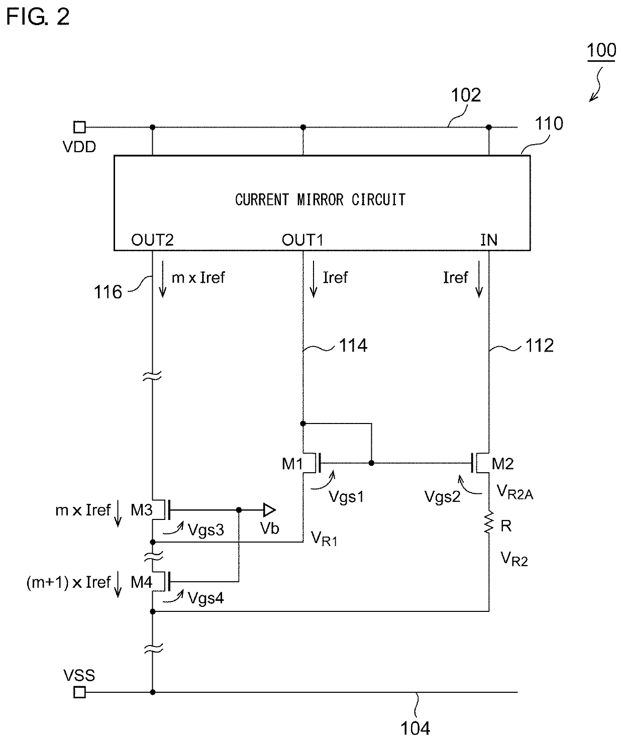
[0067]FIG. 2 is a circuit diagram of a reference current source 100 according to a first embodiment. The reference current source 100 includes a first transistor M1, a second transistor M2, a third transistor M3, a fourth transistor M4, a current mirror circuit 110, and a resistance R.
[0068]The first transistor M1 and the second transistor M2 are NMOS transistors (FET), and the control terminals (that is, gates) thereof are coupled to each other. In addition, the gate and the drain of the first transistor M1 are coupled.
[0069]The current mirror circuit 110 copies a current Iref flowing through a first path112 including the second transistor M2 and supplies the same amount of current to the second path 114 including the first transistor M1. In addition, the current mirror circuit 110 supplies a current m×Iref obtained by multiplying the current Iref of the first path 112 by a predetermined coefficient (m times) to a third path 116.
[0070]The third transistor M3 is a NMOS transistor an...
example 1.1
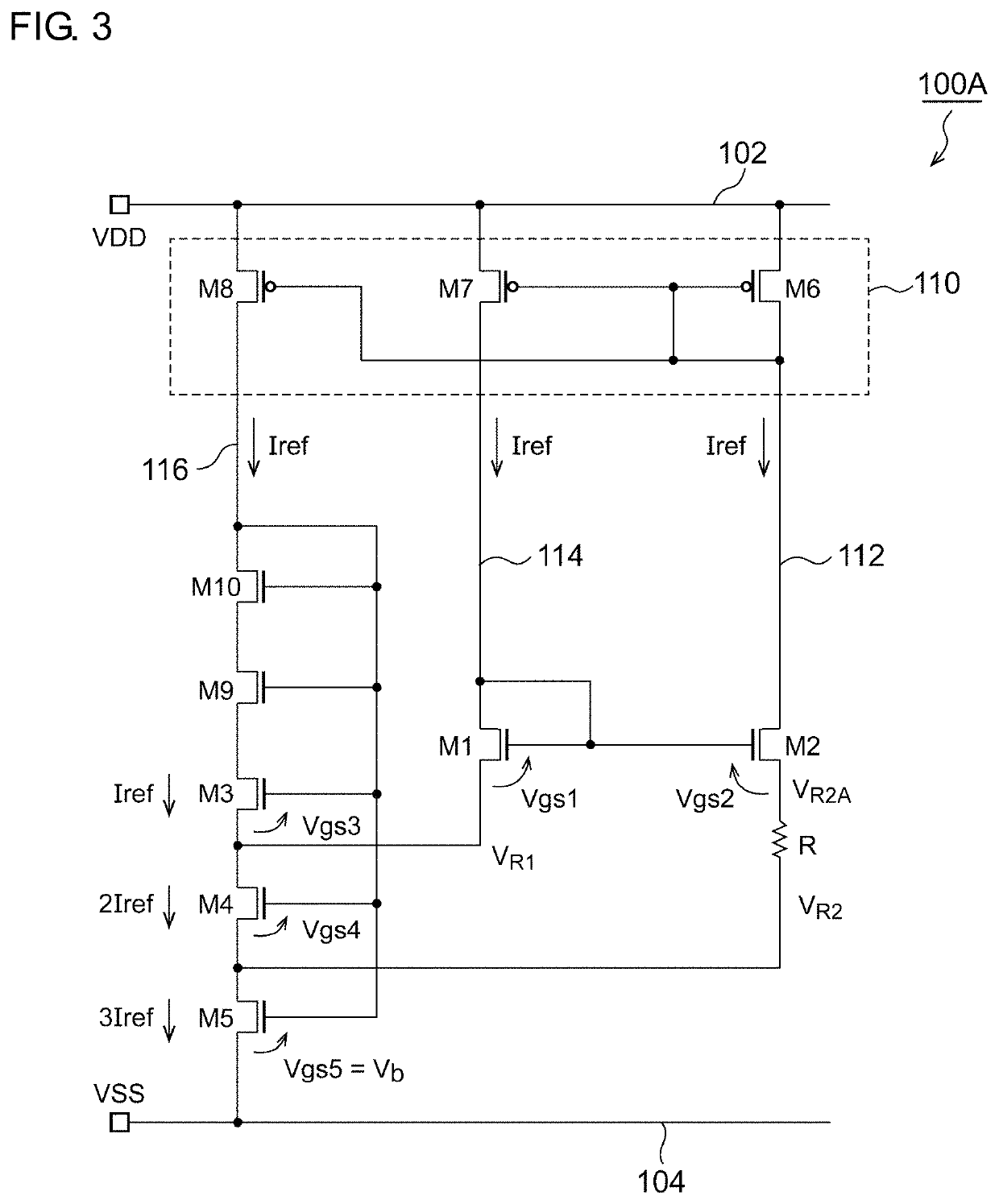
[0095]FIG. 3 is a circuit diagram of a reference current source 100A according to Example 1.1. The reference current source 100A according to Example 1.1 includes a fifth transistor M5. The fifth transistor M5 is provided on the low potential side from the fourth transistor M4 on the third path 116, and one end (source) thereof is coupled to a grounding line 104. The total current (m+2)×Iref of the current (m+1)×Iref flowing through the fourth transistor M4 and the current Iref flowing through the second transistor M2 flows to the fifth transistor M5.
[0096]The voltage Vgs5 of the control terminal (that is, a gate) of the fifth transistor M5 is applied as the bias voltage Vb in FIG. 2 to the gates of the transistors M3 and M4.
[0097]The current mirror circuit 110 includes a sixth transistor M6, a seventh transistor M7, and an eighth transistor M8 which are PMOS transistors. The gates of the sixth transistor M6 to the eighth transistor M8 are coupled to each other in common, and the so...
example 1.2
[0108]FIG. 6 is a circuit diagram of a reference current source 100B according to Example 1.2. In Example 1.2, the transistor M5 of FIG. 3 is omitted, and the source of the fourth transistor M4 is coupled to the grounding line 104. That is, the gate-source voltage Vgs4 of the fourth transistor M4 corresponds to the bias voltage Vb.
[0109]The first embodiment has been described for exemplary purposes only. It is understood by those skilled in this art that various modifications may be made in the combination of the components and the processing processes, and such modifications are also within the range of the invention. Hereinafter, the description will be given about such modifications.
PUM
 Abstract
Description
Claims
Application Information
 - R&D
- Intellectual Property
- Life Sciences
- Materials
- Tech Scout
- Unparalleled Data Quality
- Higher Quality Content
- 60% Fewer Hallucinations
Browse by: Latest US Patents, China's latest patents, Technical Efficacy Thesaurus, Application Domain, Technology Topic, Popular Technical Reports.
© 2025 PatSnap. All rights reserved.Legal|Privacy policy|Modern Slavery Act Transparency Statement|Sitemap|About US| Contact US: help@patsnap.com