Synchronous mirror delay circuit and synchronous mirror delay operation method

a technology of synchronous delay and synchronous mirror, which is applied in the direction of pulse technique, digital storage, instruments, etc., can solve the problems of requiring a larger current and a larger physical size, and achieve the effects of reducing current consumption, reducing current consumption, and reducing siz

Active Publication Date: 2020-02-13
WINBOND ELECTRONICS CORP
View PDF0 Cites 4 Cited by
  • Summary
  • Abstract
  • Description
  • Claims
  • Application Information

AI Technical Summary

Benefits of technology

[0008]The invention provides a synchronous mirror delay (SMD) circuit to overcome the problems described above. The SMD circuit of the invention can be applied to a large frequency bandwidth. In addition, compared with traditional SMD, the SMD circuit of the invention has lower current consumption and smaller size.

Problems solved by technology

However, in the operation of a traditional SMD circuit, the period of the external input clock signal CLKEXT cannot be known, therefore, many stages of delay units need to be configured in advance to make sure that the external input clock signal CLKEXT can still synchronize with the internal operation clock signal CLKINT, when the period of the external input clock signal CLKEXT is too slow.
However, for these multiple stages of delay units, the SMD circuit may require a larger current, and a larger physical size will be required for the manufacturing process of the SMD circuit.

Method used


Image

  • Synchronous mirror delay circuit and synchronous mirror delay operation method
  • Synchronous mirror delay circuit and synchronous mirror delay operation method
  • Synchronous mirror delay circuit and synchronous mirror delay operation method

Examples


Embodiment Construction

[0025]The following description is of the best-contemplated mode of carrying out the invention. This description is made for the purpose of illustrating the general principles of the invention and should not be taken in a limiting sense. The scope of the invention is best determined by reference to the appended claims.

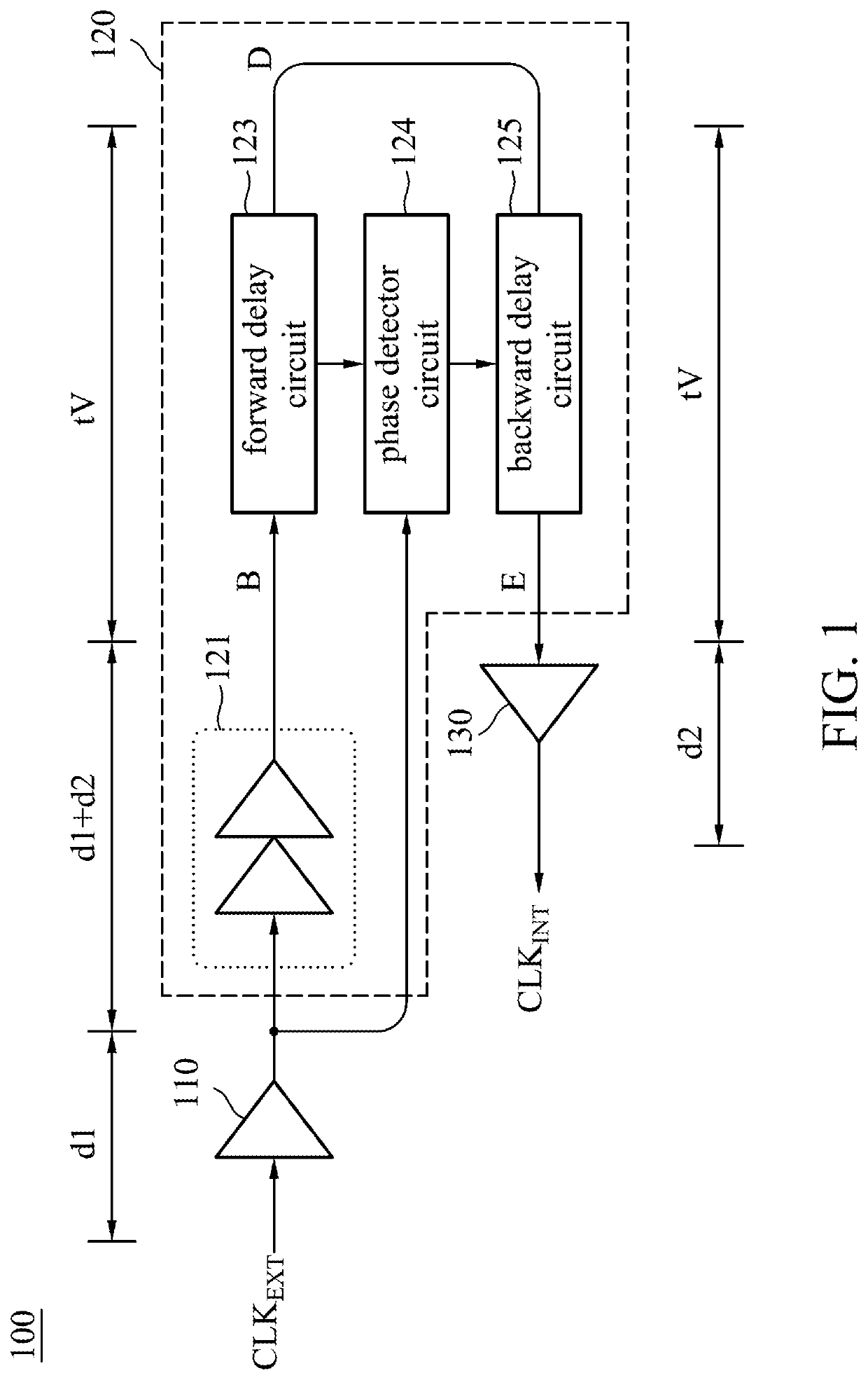
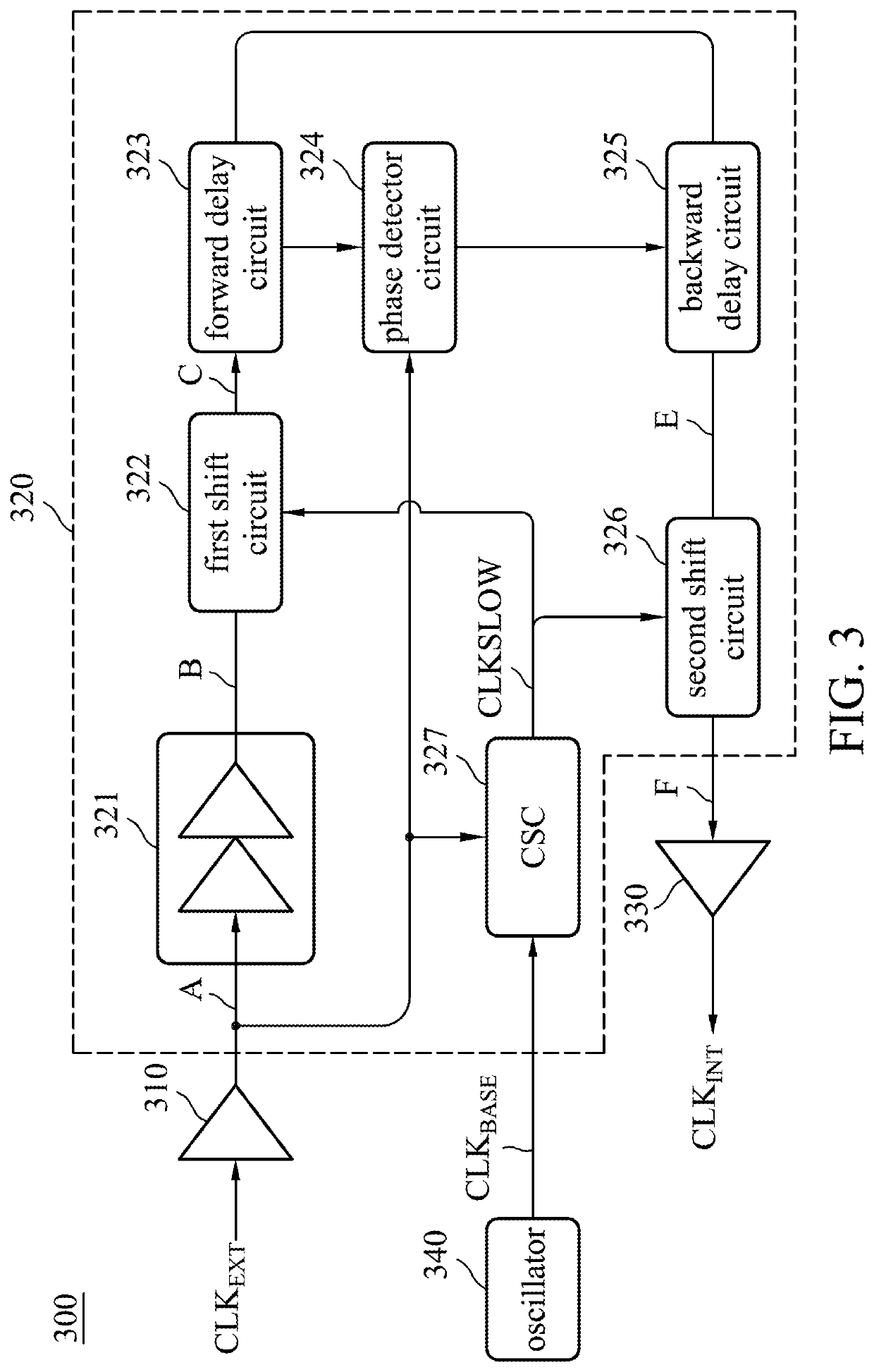
[0026]FIG. 3 is a circuit diagram of a memory circuit 300 according to an embodiment of the invention. As shown in FIG. 3, the memory circuit 300 may comprise an input buffer 310, a synchronous mirror delay (SMD) circuit 320, a clock driver 330 and an oscillator 340.

[0027]As shown in FIG. 3, the SMD circuit 320 may comprise a delay monitor circuit (DMC) 321, a first shift circuit 322, a forward delay circuit 323, a phase detector circuit 324, and a backward delay circuit 325, a second shift circuit 326 and a clock-frequency-checker (CSC) circuit 327. The DMC may comprise a dummy input buffer and a dummy clock driver. The forward delay circuit 323, the phase detector ci...


PUM


Abstract

A synchronous mirror delay (SMD) circuit is provided in the invention. The SMD circuit includes a delay monitor circuit (DMC), a forward delay circuit, a first shift circuit, a backward delay circuit, a second shift circuit and a clock-frequency-checker (CSC) circuit. The CSC circuit is coupled to the first shift circuit and the second shift circuit. The CSC circuit determines whether the frequency of the external input clock signal is slower than the frequency of the reference clock signal to generate a judgment result, and the CSC circuit transmits the judgment result to the first shift circuit and the second shift circuit. The first shift circuit and the second shift circuit determine whether to delay the external input clock signal according to the judgment result.

Description

CROSS REFERENCE TO RELATED APPLICATIONS[0001]This application claims priority of TW Patent Application No. 107127947 filed on Aug. 10, 2018, the entirety of which is incorporated by reference herein.BACKGROUND OF THE INVENTIONField of the Invention[0002]The invention generally relates to synchronous mirror delay (SMD) circuit technology, and more particularly, to SMD technology applied to the large frequency bandwidth.Description of the Related Art[0003]Synchronous mirror delay (SMD) circuits are widely applied in the designs of the integrated circuits. For different external input clock signals of an integrated circuit, the SMD circuit may be configured to synchronize the external input clock signal and the internal operation clock signal of the integrated circuit.[0004]As shown in FIG. 1, the integrated circuit 100 may comprise an input buffer 110, an SMD circuit 120 and a clock driver 130. In addition, the SMD circuit 120 may comprise a delay monitor circuit (DMC) 121, a forward ...

Claims


Application Information

Patent Timeline
Patent Type & Authority Applications(United States)
IPC IPC(8): H03K5/135G11C7/22
CPCH03K5/135G11C7/222G11C7/225
Inventor HO, WEN-CHIAO
Owner WINBOND ELECTRONICS CORP
Why Eureka
Try Eureka