
Pixel circuit

a pixel circuit and circuit technology, applied in the field of electronic circuits, can solve the problems of side effects and inaccurate image data of the pixel unit, and achieve the effects of reducing leakage current, reducing leakage path, and reducing signal errors caused by side effects

Active Publication Date: 2020-03-05
HIMAX IMAGING LIMITED
View PDF5 Cites 2 Cited by
  • Summary
  • Abstract
  • Description
  • Claims
  • Application Information

AI Technical Summary

Benefits of technology

The present invention provides a pixel circuit that reduces signal errors caused by leakage current. This is achieved by designing a storage node that minimizes the path through which the PD signal can leak.

Problems solved by technology

As a result, some side effects may be introduced.
For example, the image data of this pixel unit may be inaccurate due to a leakage current.

Method used


Image

  • Pixel circuit
  • Pixel circuit
  • Pixel circuit

Examples


Embodiment Construction

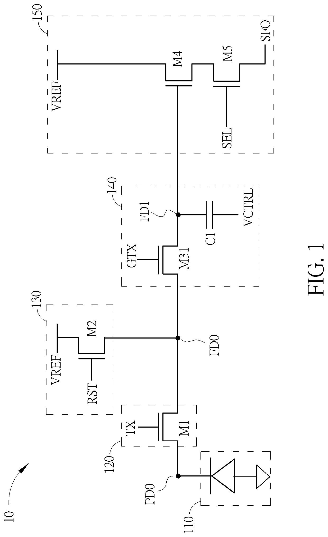
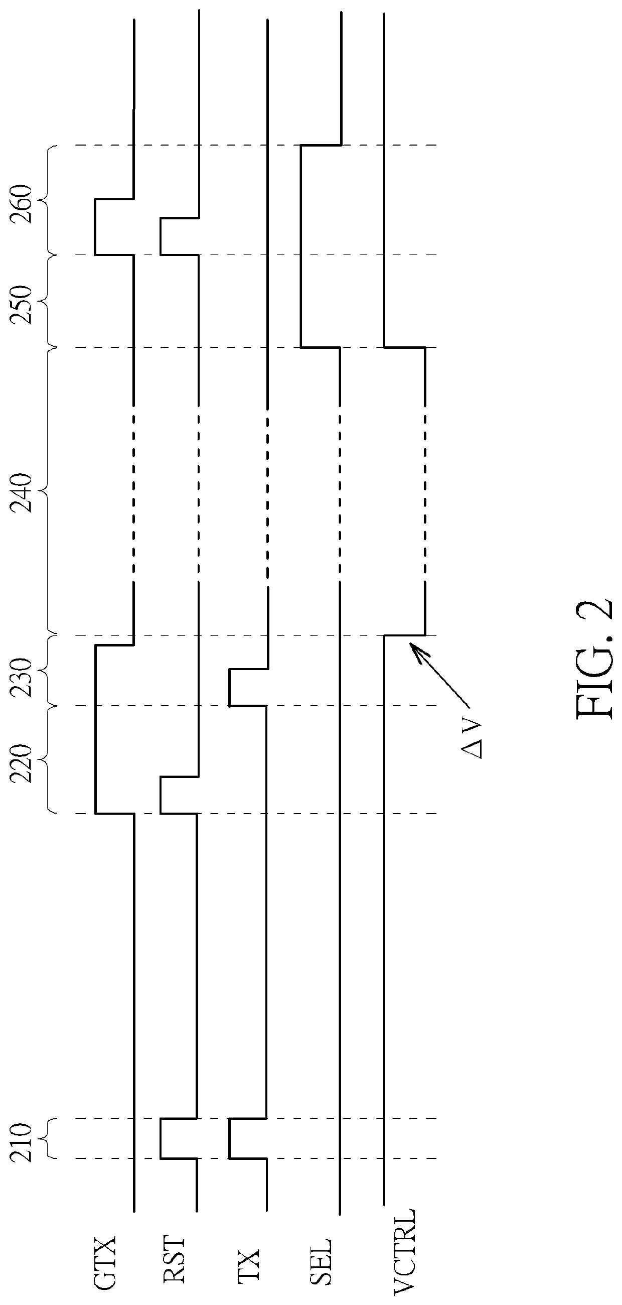
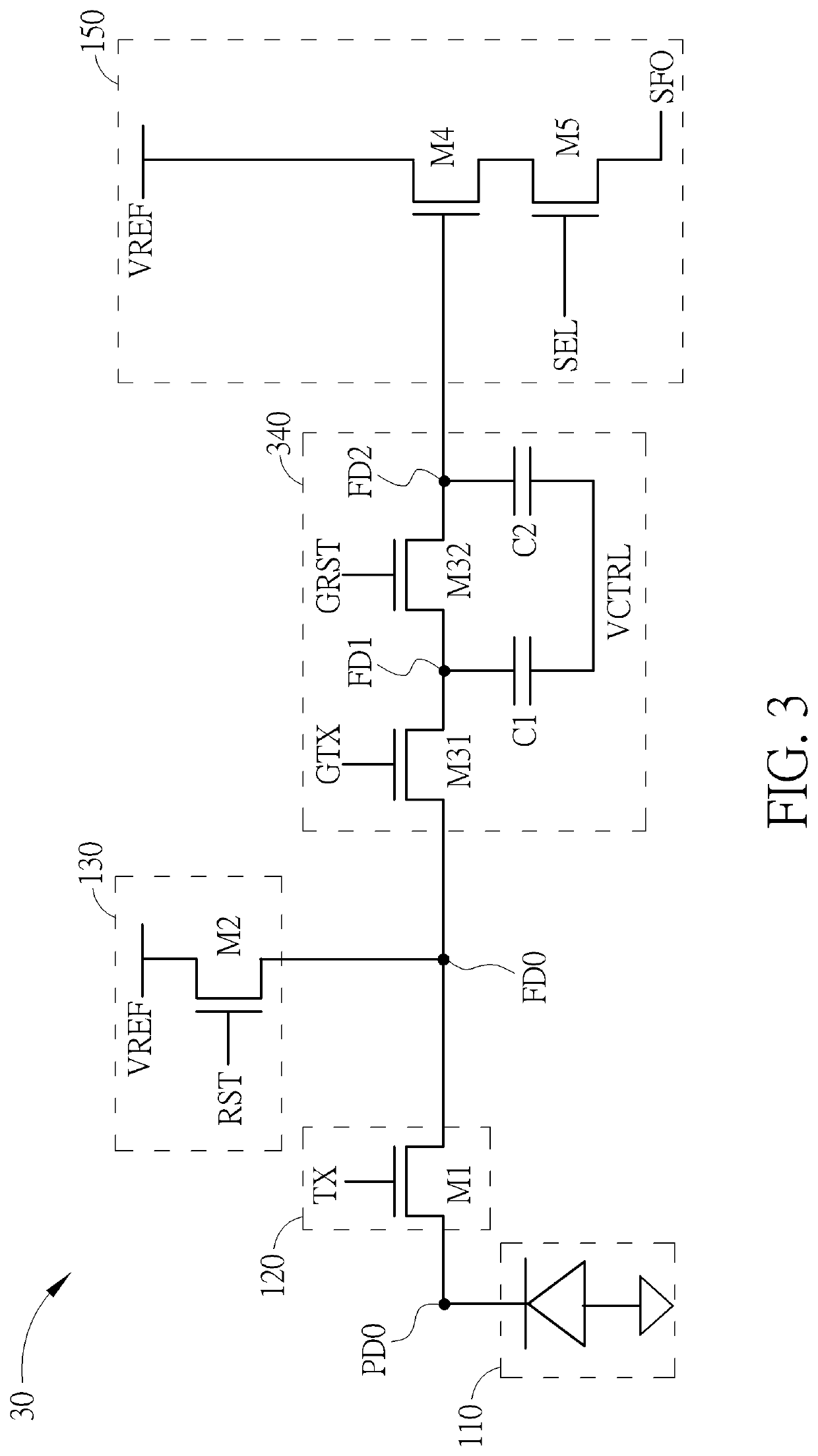
[0020]FIG. 1 is a diagram illustrating a pixel circuit 10 according to an embodiment of the present invention. The pixel circuit 10 may comprise a PD 110, a transmission circuit 120, a reset circuit 130, a signal storage circuit 140 and a buffer circuit 150. The transmission circuit 120 is coupled between the PD 110 and an FD node FD0, the reset circuit 130 is coupled to the FD node FD0, the signal storage circuit 140 is coupled to the FD node FD0, and the buffer circuit 150 is coupled to the signal storage circuit 140.

[0021]In this embodiment, the PD 110 is coupled to the transmission circuit 120 through a PD node PD0, and the PD 110 may accumulate charges on the PD node PD0 in response to incident radiation, to generate a PD signal on the PD node PD0. The transmission circuit 120 may comprise at least one transistor such as a transistor M1, where a gate terminal of the transistor M1 is coupled to a control signal TX. The reset circuit 130 may comprise at least one transistor such ...


PUM


Abstract

A pixel circuit is disclosed. The pixel circuit includes a photodiode (PD), a transmission circuit, a reset circuit, a signal storage circuit and a buffer circuit. The transmission circuit is coupled between the PD and an ordinary floating diffusion (FD) node. The reset circuit is coupled to the ordinary FD node. The signal storage circuit is coupled to the ordinary FD node. The buffer circuit is coupled to the signal storage circuit. The signal storage circuit may store a PD signal on a specific node having a reduced leakage path in comparison with the ordinary FD node during a holding phase of the pixel circuit, wherein the holding phase is a time interval starting from a first time point at which the PD signal is stored on the specific node and ending at a second time point at which the pixel circuit is selected for performing a read-out operation.

Description

CROSS REFERENCE TO RELATED APPLICATIONS[0001]This application claims the benefit of U.S. provisional application No. 62 / 724,042, which was filed on Aug. 29, 2018, and is included herein by reference.BACKGROUND OF THE INVENTION1. Field of the Invention[0002]The present invention is related to electronic circuits, and more particularly, to a pixel circuit.2. Description of the Prior Art[0003]In comparison with a rolling shutter image sensor, all pixel units of a global shutter image sensor obtain image data in a same time interval, rather than row by row. For some considerations, however, the image data of respective pixel units are read out sequentially rather than concurrently. Therefore, an in-pixel storage mechanism is required, in order to hold image data of a certain pixel unit until this pixel unit is selected for performing a read-out operation.[0004]The above mechanisms for global shutter still have some disadvantages. For example, as time intervals of respective pixel units ...

Claims


Application Information

Patent Timeline
Patent Type & Authority Applications(United States)
IPC IPC(8): H04N5/3745H04N5/378
CPCH04N5/37452H04N5/353H04N5/378G09G3/20H04N25/78H01L27/14641H04N25/771H04N25/616H04N25/77H04N25/75H04N25/53
Inventor OH, HACK SOOCHEUNG, YU HIN DESMONDKIM, KIHONG
Owner HIMAX IMAGING LIMITED
Learn More