

Shield gate mosfet and method for fabricating the same
- Summary
- Abstract
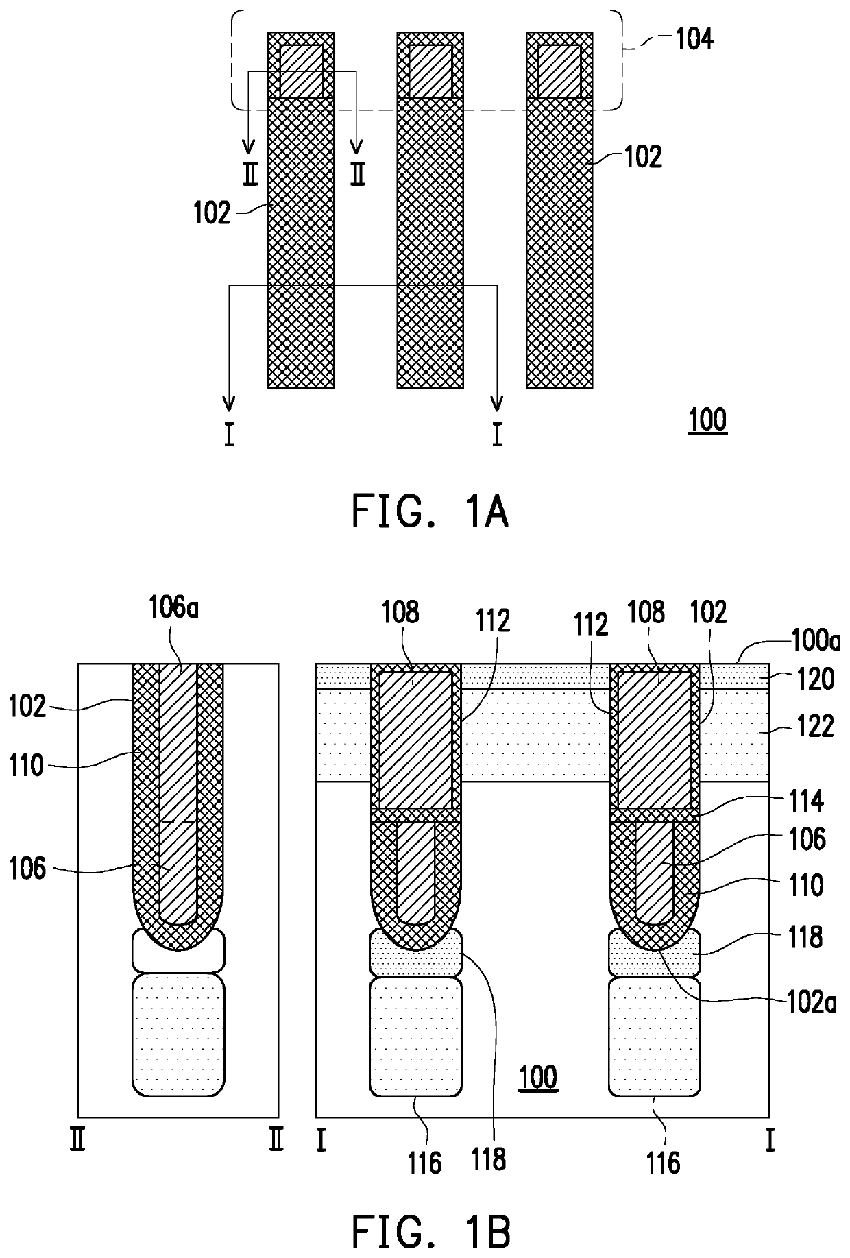
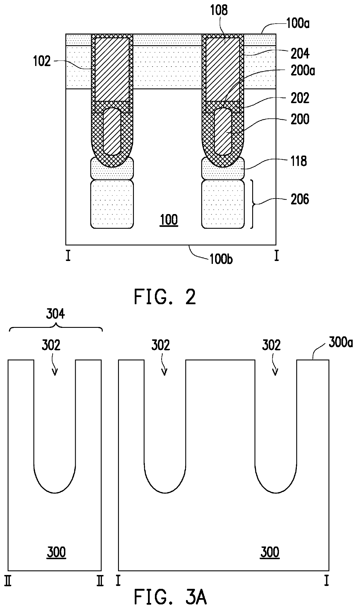
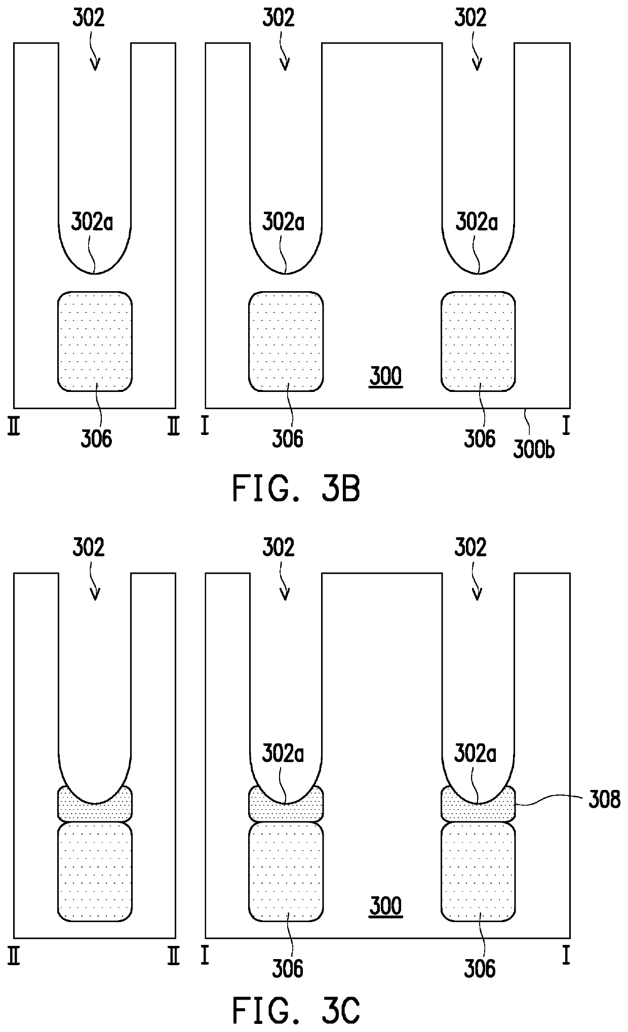
- Description
- Claims
- Application Information
AI Technical Summary
Benefits of technology
Problems solved by technology
Method used
Image

Examples
experimental example 1
SIMULATION EXPERIMENTAL EXAMPLE 1
[0054]The simulated structure is the shield gate MOSFET (EPI resistance is 0.35 Ω·cm / thickness 4 μm) shown in FIG. 1B, and a 150 V DG breakdown voltage is simulated, wherein the first doped region is P type, and the second doped region is N type, the doping dosage of the first doped region is a variable, and the depth is about 0.5 μm to 1.5 μm. The depth of the second doped region is about 0.5 μm or less and the doping dosage is 2E11 cm−2, which are shown in FIG. 4 together with the simulation results (BVDss).
[0055]As may be seen from FIG. 4, the structure of the disclosure has a breakdown voltage higher than 152 V; when the doping dosage of the first doped region is 4E12 cm−2 to 5E12 cm−2, the breakdown voltage thereof is higher than 160 V.
PUM
 Abstract
Description
Claims
Application Information