ScAlN/GaN double-barrier resonant tunneling diode and manufacturing method thereof

A resonant tunneling and diode technology, which is applied in the direction of diodes, semiconductor/solid-state device manufacturing, electrical components, etc., can solve the problem of increasing the peak voltage of the differential negative resistance effect of resonant tunneling and device power consumption, and reducing the electron tunneling under reverse bias. Problems such as wear probability and uneven distribution of dislocations in the active area of ​​the device can be achieved to reduce the consistency of device performance, improve the differential negative resistance effect of the device, and improve the stability and reliability of the device

Active Publication Date: 2021-07-09
XIDIAN UNIV
View PDF8 Cites 2 Cited by
  • Summary
  • Abstract
  • Description
  • Claims
  • Application Information

AI Technical Summary

Problems solved by technology

[0005] One is that there is a large lattice mismatch in the AlGaN / GaN / AlGaN double-barrier quantum well. The active region of the device has a high density of dislocations, and the interface of the quantum well is rough and uneven. These material defects act as scattering centers and leakage channels, and ultimately reduce the device The peak current increases the valley current to degrade the differential negative resistance effect;
[0006] The second is that there is a strong piezoelectric polarization and spontaneous polarization electric field in the AlGaN / GaN / AlGaN double barrier quantum well, which modulates the band structure of the quantum well and affects the transport of the device under forward and reverse bias. characteristics, producing an asymmetrical differential negative resistance effect;
[0007] The third is that there is a wide depletion region on the collector side of the GaN resonant tunneling diode, which reduces the probability of electron tunneling under reverse bias and weakens the differential negative resistance characteristics under reverse bias;
[0008] Fourth, the ohmic contact resistance of the collector is high, and the series resistance of the device is high, which increases the peak voltage of the resonance tunneling differential negative resistance effect and the power consumption of the device;
[0009] Fifth, the distribution of dislocations in the active area of ​​the device is uneven, resulting in unstable device performance and low reliability. The device performance decreases with the increase in size, and the performance consistency of the same size device is poor.

Method used


Image

  • ScAlN/GaN double-barrier resonant tunneling diode and manufacturing method thereof
  • ScAlN/GaN double-barrier resonant tunneling diode and manufacturing method thereof
  • ScAlN/GaN double-barrier resonant tunneling diode and manufacturing method thereof

Examples


Embodiment 1

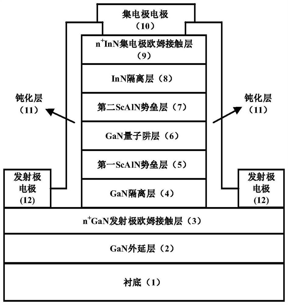
[0059] Embodiment 1, on a self-supporting gallium nitride substrate, a Sc 0.18 al 0.82 N barrier layer and n + InN collector ohmic contact layer doping concentration is 1x10 20 cm -3 ScAlN / GaN double barrier resonant tunneling diode.

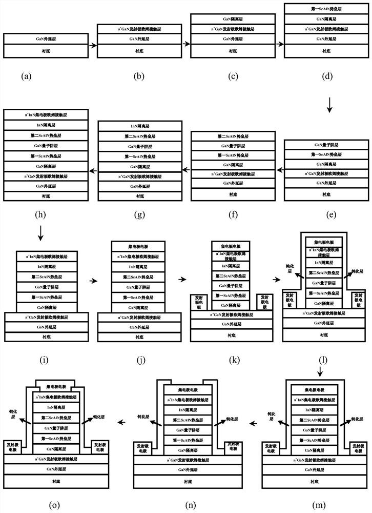
[0060] Step 1, growing a GaN epitaxial layer, such as image 3 (a).

[0061] A GaN epitaxial layer with a thickness of 1500nm is grown on a self-supporting gallium nitride substrate by molecular beam epitaxy.

[0062] The process conditions used to grow the GaN epitaxial layer are: the temperature is 700°C, the equilibrium vapor pressure of the gallium beam is 8.0×10 - 7 Torr, the flow rate of nitrogen gas is 2.3sccm, and the power of the nitrogen plasma RF source is 375W.

[0063] Step two, grow n + GaN emitter ohmic contact layer, such as image 3 (b).

[0064] Using the molecular beam epitaxy method, the thickness of the GaN epitaxial layer is 100nm, and the doping concentration is 1x10 20 cm -3 the n + GaN emitter ohmic contac...

Embodiment 2

[0135] Embodiment two, on the sapphire substrate, making adopts Sc 0.2 al 0.8 N barrier layer and n + InN collector ohmic contact layer doping concentration is 5x10 19 cm -3 ScAlN / GaN double barrier resonant tunneling diode.

[0136] Step 1, grow GaN epitaxial layer, such as image 3 (a).

[0137] Using the metal-organic chemical vapor deposition method, under the process conditions of temperature 1050°C, pressure 40Torr, ammonia flow rate 2000sccm, gallium source flow rate 120sccm, hydrogen flow rate 3000sccm, on a sapphire substrate, the growth thickness is 3000nm GaN epitaxial layer.

[0138] Step 2, grow n + GaN emitter ohmic contact layer, such as image 3 (b).

[0139] Using the molecular beam epitaxy method, at a temperature of 720°C, the equilibrium vapor pressure of the gallium beam is 8.5×10 -7 Torr, the silicon beam equilibrium vapor pressure is 3.2×10 -8 Torr, the nitrogen gas flow rate is 2.3sccm, and the nitrogen plasma RF source power is 375W, the thi...

Embodiment 3

[0182] Embodiment three, on the silicon substrate, make and adopt Sc 0.15 Al 0.85 N barrier layer and n + InN collector ohmic contact layer doping concentration is 1x10 19 cm -3 ScAlN / GaN double barrier resonant tunneling diode.

[0183] Step A, growing a GaN epitaxial layer, such as image 3 (a).

[0184] Using the metal-organic chemical vapor deposition method, under the process conditions of temperature 1100°C, pressure 40Torr, ammonia gas flow rate 2000 sccm, gallium source flow rate 100 sccm, hydrogen gas flow rate 3000 sccm, on Si substrate, the growth thickness is 4000nm GaN epitaxial layer.

[0185] Step B, grow n + GaN emitter ohmic contact layer, such as image 3 (b).

[0186] Using molecular beam epitaxy, at a temperature of 680°C and a gallium beam equilibrium vapor pressure of 7.5×10 -7 Torr, silicon beam equilibrium vapor pressure is 3.0×10 -8 Under the process conditions of Torr, nitrogen gas flow rate of 2.3sccm, and nitrogen plasma RF source power o...


PUM

PropertyMeasurementUnit
thicknessaaaaaaaaaa
thicknessaaaaaaaaaa
thicknessaaaaaaaaaa

Abstract

The invention discloses an ScAlN/GaN double-barrier resonant tunneling diode and a manufacturing method thereof. The ScAlN/GaN double-barrier resonant tunneling diode mainly solves the problems that an existing gallium nitride resonant tunneling diode is low in peak current, small in peak-valley current ratio and asymmetric in differential negative resistance effect. The ScAlN/GaN double-barrier resonant tunneling diode comprises a substrate, a GaN epitaxial layer, an n+GaN emitter ohmic contact layer, a GaN isolation layer, a first barrier layer, a GaN quantum well layer, a second barrier layer, an isolation layer, a collector ohmic contact layer and a collector electrode from bottom to top, wherein the two barrier layers both adopt ScAlN which has an Sc component range of 15% to 20% and a thickness of 1-3 nm and is identical in the Sc component and thickness; the isolation layer is made of InN with a thickness of 2-4 nm; and the collector ohmic contact layer adopts n+InN. The ScAlN/GaN double-barrier resonant tunneling diode is high in peak current, large in peak-valley current ratio, capable of achieving forward and reverse symmetrical differential negative resistance effect, high in working frequency and output power and applicable to a high-frequency terahertz radiation source and a high-speed digital circuit.

Description

technical field [0001] The invention belongs to the technical field of semiconductor devices, and in particular relates to a ScAlN / GaN double potential barrier resonant tunneling diode, which can be used for high-frequency terahertz radiation sources and high-speed digital circuits. Background technique [0002] Resonant tunneling diode is a vertical structure quantum effect device, which has the characteristics of differential negative resistance, low junction capacitance, short carrier transport time, unipolar transport, etc., and its working frequency can reach terahertz frequency band. Oscillators prepared based on resonant tunneling diode devices have the advantages of high frequency and low power consumption, and are one of the ways to realize terahertz radiation sources. They are widely used in security detection, spectral imaging, high-speed wireless communication and circuit design. With the advancement of material growth technology and device fabrication process, I...

Claims


Application Information

Patent Timeline
Patent Type & Authority Applications(China)
IPC IPC(8): H01L29/88H01L29/06H01L29/12H01L29/20H01L29/205H01L29/36H01L29/45H01L21/329
CPCH01L29/882H01L29/0607H01L29/0684H01L29/0649H01L29/122H01L29/2003H01L29/205H01L29/36H01L29/452H01L29/66219
Inventor 薛军帅刘芳张进成郝跃孙志鹏李蓝星姚佳佳杨雪妍张赫朋
Owner XIDIAN UNIV
Why Eureka
Try Eureka