Transistor structure with multiple halo implants having epitaxial layer over semiconductor-on-insulator substrate

a technology of semiconductor-on-insulator substrate and transistor, which is applied in the direction of transistors, semiconductor devices, electrical devices, etc., can solve the problems of affecting the functionality, yield and reliability of transistors, physical dimensions pose certain complexities, and severely affect the specific characteristics of transistors, so as to reduce process variability, reduce process variability, and minimize the effect of transistor resistan

Active Publication Date: 2020-04-30
SAHA SAMAR K
View PDF0 Cites 2 Cited by
  • Summary
  • Abstract
  • Description
  • Claims
  • Application Information

AI Technical Summary

Benefits of technology

[0007]A transistor structure having an epitaxial layer deposited over the implanted substrate in order to reduce process variability. In particular, the epitaxial layer is able to be un-doped (or lightly doped via up-diffusion from the implanted substrate) and used to form the channel for the transistor structure. As a result, this use of un-doped epitaxial layer provides the benefit of reducing process variability (e.g. random dopant fluctuations) and thus the transistor performance variability despite the small physical size of the transistors. The substrate, can be a semiconductor-on-insulator substrate, such a silicon-on-insulator (SOI), having a buried insulator layer within the substrate. Above the buried insulator, there can be a well that extends to a first depth, a threshold voltage-adjust implant of the same polarity at a second depth shallower than the first depth, a shallow halo implant of the first polarity defined at a second depth shallower than the first depth and deeper than the second depth, and a deep halo implant of the same polarity as the substrate defined at a fourth depth deeper than the third depth. The shallow halo implant and the deep halo implant allow a peak concentration of substrate impurities at a level below the gate such that the resistance of the transistor is minimized along with the threshold voltage, threshold voltage fluctuations, short channel effects, and leakage current in the transistor. The transistor structure can be an n-channel metal oxide semiconductor (NMOS), p-channel metal oxide semiconductor (PMOS) or other types of transistor structures. In some embodiments, the structure is able to be characterized as a buried halo (BH) metal-oxide-semiconductor field effect transistor (BH-MOSFET).
[0008]In some embodiments, a buried insulator can be a relatively thin layer, and a body region formed below the buried insulator can be biased to operate the transistor in a double-gate mode. This can enable greater gate control, and improved on-off operation, as compared to conventional transistors of the same general channel size.

Problems solved by technology

Although there is a growing demand to scale transistor gate lengths to about 22 nm (i.e., 0.022 micron) and below for more demanding and compact digital circuit applications, such physical dimensions pose certain complexities.
In particular, as transistors decrease in size the effects of process variability on the transistors continue to increase such that it is able to severely impact the functionality, yield and reliability of the transistors.
For example, highly random effects that occur during processing of the transistors, such as random dopant fluctuations, oxide thickness variation and line-edge / width roughness, cause variability in the specific characteristics of each transistor.
Another problem caused by the demand for smaller physical dimensions is the transistor off-state leakage current.
However, for small gate length devices, even in the off-state, the space-charge region near the drain touches the source in a deeper place where the gate bias cannot control the potential, resulting in leakage current from the source to drain via the space-charge region.
Yet another problem with the manufacturing of sub-22 nm transistors is the susceptibility to punch through.
Since sub-22 nm transistors are pushing the limits on semiconductor manufacturing, transistor shorting or leakage due to punch through is a problem that needs to be addressed.

Method used


Image

  • Transistor structure with multiple halo implants having epitaxial layer over semiconductor-on-insulator substrate
  • Transistor structure with multiple halo implants having epitaxial layer over semiconductor-on-insulator substrate
  • Transistor structure with multiple halo implants having epitaxial layer over semiconductor-on-insulator substrate

Examples


Embodiment Construction

:

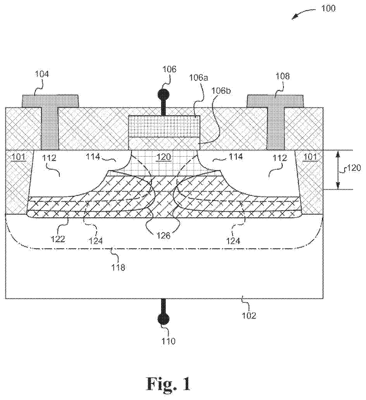
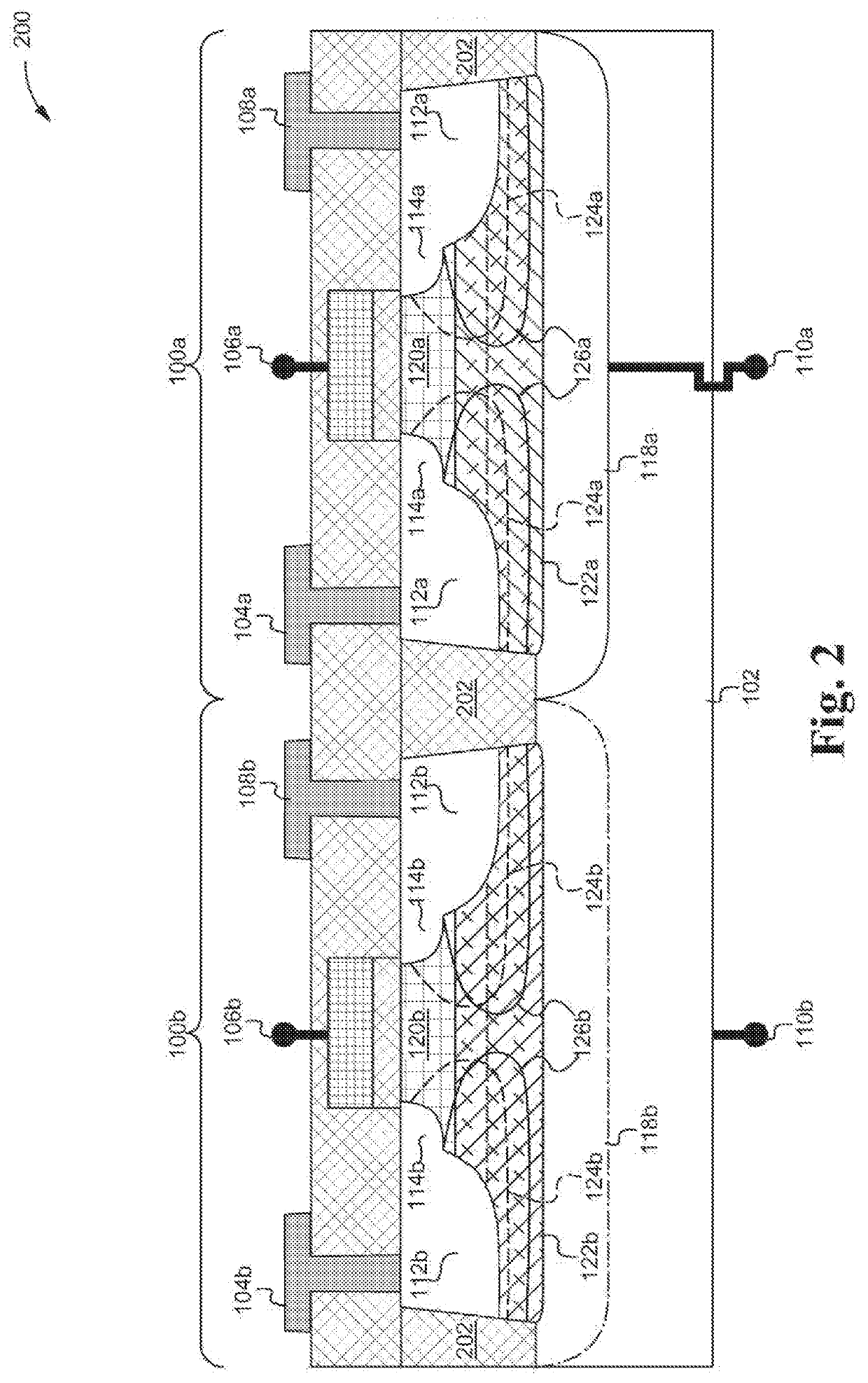
[0026]Embodiments of the application are directed systems, devices and methods of making a transistor structure having an epitaxial layer on top of a doped substrate such that the epitaxial layer is able to be un-doped or lightly doped thereby reducing process variability (e.g. random dopant variability in the channel and / or other regions) in the transistor structure. In particular, the epitaxial layer enables the transistor structure to have optimized source-drain and / or channel regions to mitigate the risk of process variability in device and circuit performance despite shrinking transistor dimensions. The transistor structure is also able to comprise a plurality of halo regions, formed in a semiconductor-on-insulator substrate, at varying depths that enable a peak concentration of substrate impurities at a level below the gate such that the resistance of the transistor is minimized along with the threshold voltage, threshold voltage fluctuations, short channel effects, and leaka...


PUM

PropertyMeasurementUnit
thicknessaaaaaaaaaa
thicknessaaaaaaaaaa
thicknessaaaaaaaaaa

Abstract

A transistor structure can include a semiconductor-on-insulator substrate that includes an upper substrate region separated from a lower substrate region by a buried insulator. Shallow halo implant regions can be formed in an upper substrate region having a peak concentration at a first depth within the upper substrate region. Deep halo implant regions can be formed in the upper substrate region having a peak concentration at a second depth lower than the first depth. An epitaxial layer can be formed on top of the upper substrate region and below the control gate. Source and drain regions both of a second conductivity type formed in at least the epitaxial layer. In some embodiments, a lower substrate region can be biased for a double-gate effect.

Description

RELATED APPLICATIONS[0001]This application is a continuation-in-part of U.S. patent application Ser. 2No. 15 / 083,172, filed Mar. 28, 2016, and entitled, “Transistor Structure and Fabrication Methods with an Epitaxial Layer Over Multiple Halo Implants”, which is a divisional of U.S. patent application Ser. No. 14 / 229,102, filed Mar. 28, 2014, and entitled, “Transistor Structure and Method with an Epitaxial Layer Over Multiple Halo Implants,” issued as U.S. Pat. No. 9,299,702 on Mar. 29, 2016, which claims priority under 35 U.S.C. 119 (e) of U.S. Provisional Application Ser. No. 61 / 881,908, filed Sep. 24, 2013, and entitled “Transistor Structure and Method with Multiple Halo Implants and Epitaxial Layer.” This application incorporates all of these patent applications in their entirety by reference.FIELD OF THE INVENTION[0002]The present invention is generally directed to the field of transistors in semiconductor substrates. More particularly, the present invention relates to transisto...

Claims


Application Information

Patent Timeline
Patent Type & Authority Applications(United States)
IPC IPC(8): H01L21/8238H01L21/8234H01L21/324H01L21/266H01L21/265H01L21/225H01L21/205H01L21/02H01L29/10H01L27/092
CPCH01L29/1083H01L21/2053H01L21/823878H01L29/105H01L21/823468H01L21/823807H01L21/2257H01L21/0262H01L27/092H01L21/26513H01L21/324H01L21/823814H01L21/266H01L21/823418H01L21/823437H01L21/823481H01L21/84H01L27/1203H01L29/78648H01L29/6659H01L29/7833H01L29/1041H01L21/823892H01L21/02365
Inventor SAHA, SAMAR K.
Owner SAHA SAMAR K
Why Eureka
Try Eureka