Method for Microperturbation Assembly

a microperturbation and assembly technology, applied in the field of fluid assembly systems, can solve the problems of difficult to achieve the flow velocity uniformity and microcomponent dispensing scheme necessary for a high yield over the whole assembly substrate, and take several hours to complete, etc., to achieve simple and low-cost infrastructure, maximize assembly yield and speed, and cost-effectively scalable to large areas

Active Publication Date: 2020-05-07
ELUX INC
View PDF0 Cites 4 Cited by
  • Summary
  • Abstract
  • Description
  • Claims
  • Application Information

AI Technical Summary

Benefits of technology

The patent describes a way to assemble microcomponents using a low-forcing method that prevents damage to the components. This method uses a substrate with recesses to hold the components. A higher-forcing method that uses directed forcing is also described, which can increase the assembly yield and speed. The method is cost-effective and scalable to large areas. The patent also discusses options for increasing the trap rate and limiting the detrapment rate during the removal of residual components.

Problems solved by technology

However, with a display comprising millions of elements, such a process may take several hours to complete and is therefore inefficient.
Some problems yet to be addressed with conventional fluidic assembly processes are related to the distribution method over large scales, the integration of microcomponents to drive circuitry over large areas, and the potential mechanisms for the repair of defective microcomponents.
Over large scales, conventional fluidic assembly into wells is challenged by the dual requirements of maximum velocities for microcomponent capture and lesser distribution velocities to minimize the detrapment of microcomponents once they are captured.
Similarly, achieving the microcomponent dispensing scheme and flow velocity uniformity necessary for a high yield over the whole assembly substrate becomes very challenging over greater-than-centimeter scales.
Scaling this approach to large areas, however, is sufficiently difficult as to motivate alternate trapping approaches.
It allows a great deal of control, but isn't very practical for manufacturing because the top plates must be sealed and reused.
The primary weakness of the approach is related to the distance-from-impulse, in which impelled microcomponents 100 have too much momentum (A) to be captured in the wells 102.
For practical assemblies, this makes efficiently achieving a high fill near substrate edges more difficult.
Secondary weaknesses are that high forcing may damage fragile unpackaged microcomponents, and a risk of contamination exists to and from the driver—in the above example, a brush 104.

Method used


Image

  • Method for Microperturbation Assembly
  • Method for Microperturbation Assembly
  • Method for Microperturbation Assembly

Examples


Embodiment Construction

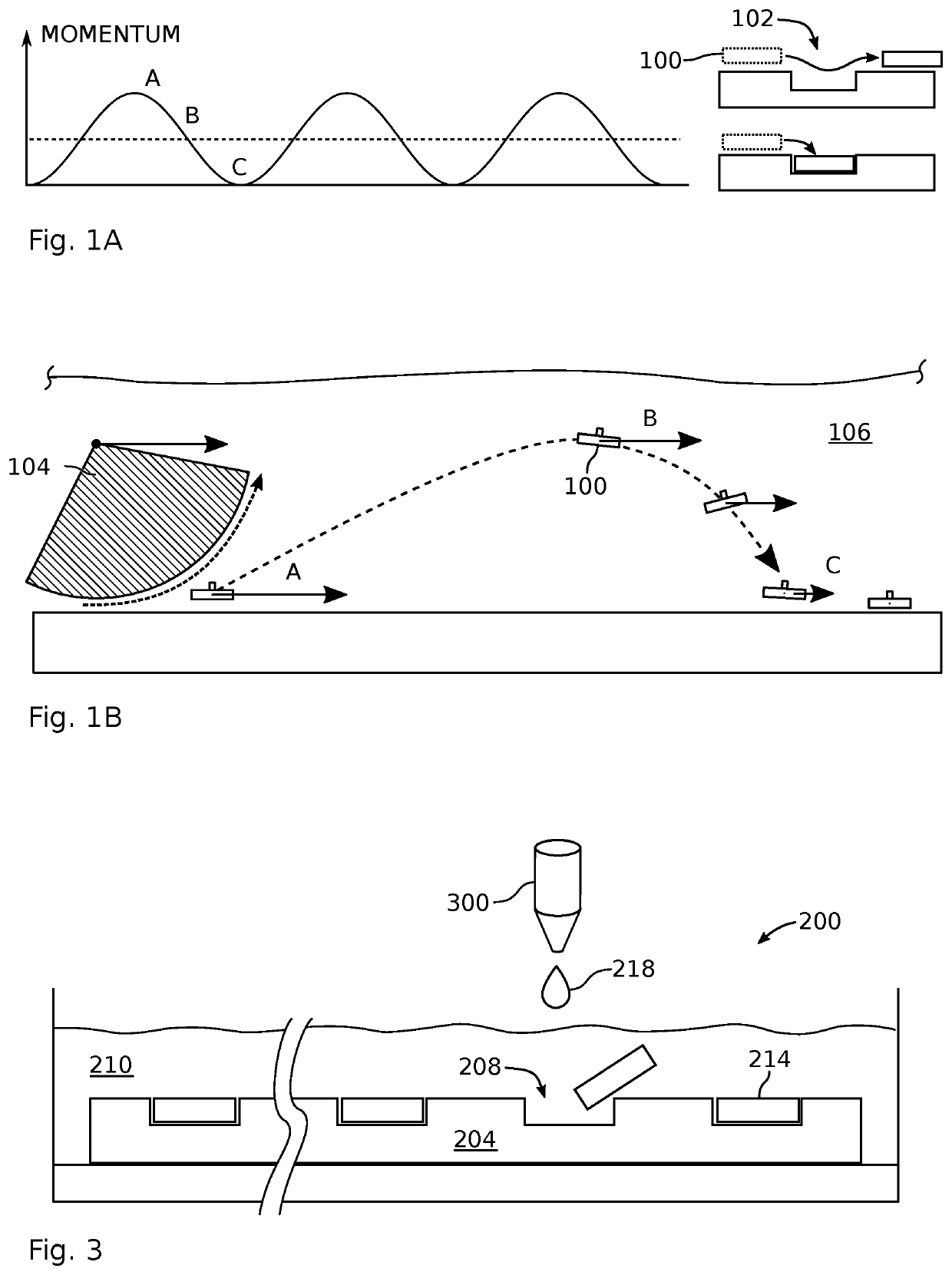
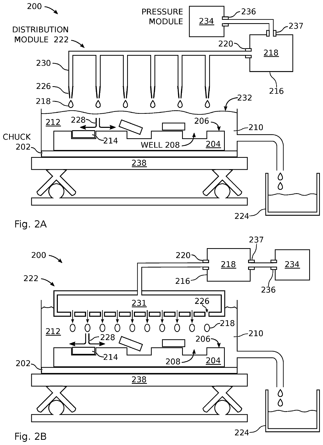
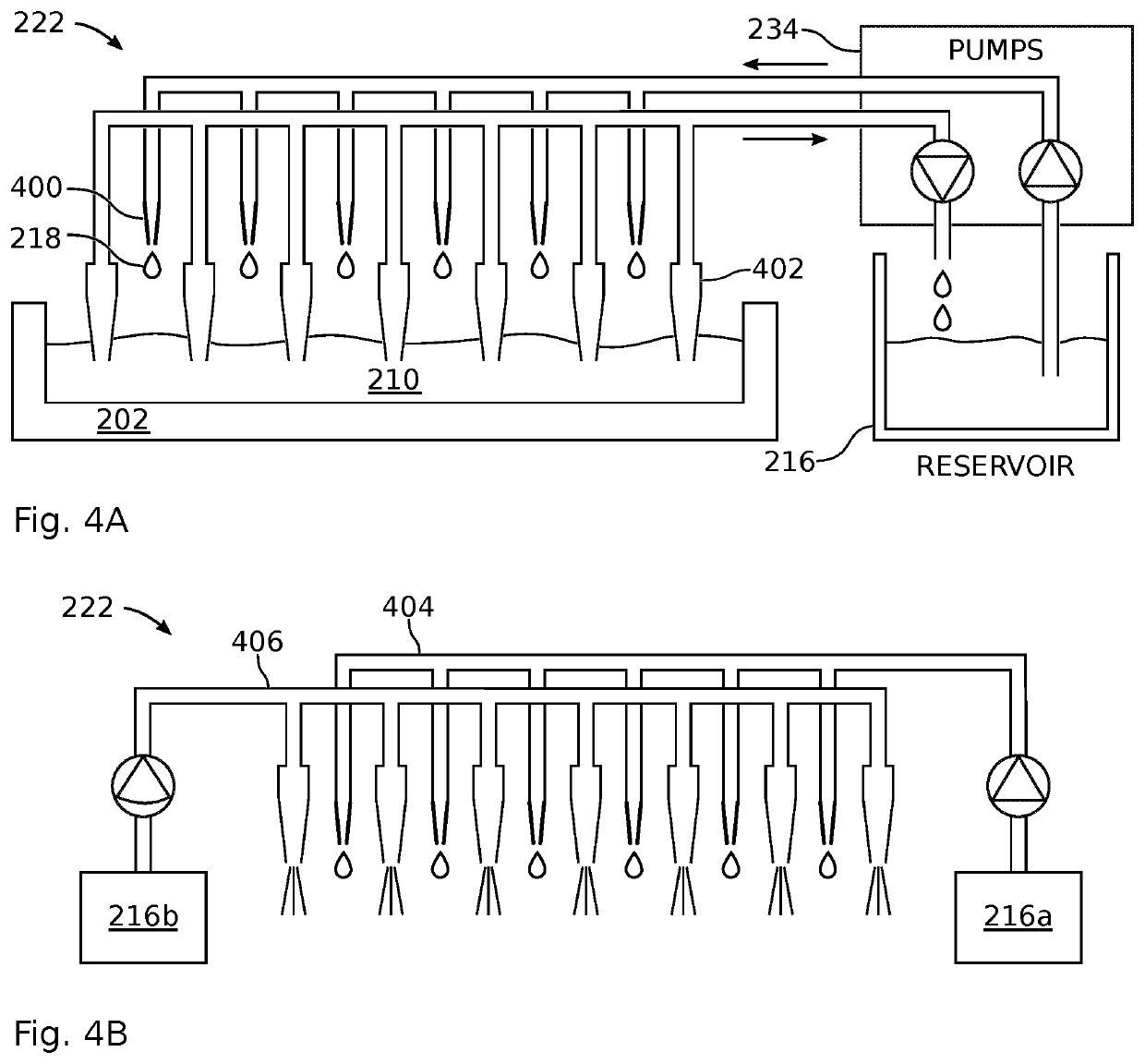
[0032]FIGS. 2A and 2B are partial cross-sectional views of an emissive substrate microperturbation fluidic assembly system. The system 200 comprises a substrate chuck 202 for engaging an emissive substrate 204. The emissive substrate 204 has a top surface 206 patterned to form an array of wells 208. A liquid suspension 210 overlies the emissive substrate top surface, comprising a first liquid 212 and emissive elements 214. The system comprises a reservoir 216, which contains a perturbation medium 218 and has an outlet port 220. The perturbation medium 218 may be the first liquid 212, a second liquid, or a gas. Optionally but not shown, a liquid perturbation medium may include emissive elements. One example of an emissive element is a light emitting diode (LED). Although not light emissive, other two-terminal surface mount elements include photodiodes, thermistors, pressure sensors, and piezoelectric devices. The emissive element may also be referred to as a surface mount emissive el...


PUM


Abstract

Microperturbation fluidic assembly systems and methods are provided for the fabrication of emissive panels. The method provides an emissive substrate with a top surface patterned to form an array of wells. A liquid suspension is formed over the emissive substrate top surface, comprising a first liquid and emissive elements. Using an array of micropores, a perturbation medium, which optionally includes emissive elements, is injected into the liquid suspension. The perturbation medium may be the first liquid, a second liquid, or a gas. A laminar flow is created in the liquid suspension along the top surface of the emissive substrate in response to the perturbation medium, and emissive elements are captured in the wells. The ejection of the perturbation medium can also be used to control the thickness of the liquid suspension overlying the top surface of the emissive substrate.

Description

RELATED APPLICATIONS[0001]Any and all applications, if any, for which a foreign or domestic priority claim is identified in the Application Data Sheet of the present application are hereby incorporated by reference under 37 CFR 1.57.BACKGROUND OF THE INVENTION1. Field of the Invention[0002]This invention generally relates to fluidic assembly systems and methods for the fabrication of emissive panels using local microperturbation features.2. Description of the Related Art[0003]The fluidic transfer of microfabricated electronic devices, optoelectronic devices, and sub-systems from a donor substrate / wafer to a large area and / or unconventional substrate provides a new opportunity to extend the application range of electronic and optoelectronic devices. For example, display pixel size light emitting diode (LED) micro structures, such as rods, fins, or disks, can be first fabricated on small size wafers and then be transferred to large panel substrate to make a direct emitting display. On...

Claims


Application Information

Patent Timeline
IPC IPC(8): B01L3/00H01L27/32H01L23/00H01L33/00H01L25/075G09G3/00
CPCH01L2924/15153H01L2224/04105H01L24/95H01L2933/0033B01L3/5027H01L25/50H01L27/3244H01L2224/73267B01L3/502784H01L25/0753H01L2224/95101H01L33/0095B01L3/50273B01L3/502715H01L24/00H01L33/005G09G3/006H01L24/29H01L2224/95085H01L2224/95123H01L2224/95133H01L2224/95136H01L2924/12041H10K59/12
Inventor SASAKI, KENJIYU, SHU-HANSCHUELE, PAUL J.
Owner ELUX INC
Why Eureka
Try Eureka