Semiconductor device having a through silicon via and methods of manufacturing the same

a silicon via and semiconductor technology, applied in the field of semiconductor devices, can solve the problems of metal contaminants attaching to the lower sidewall, semiconductor devices may have poor reliability, and failure of reliability, and achieve the effect of reducing failure of reliability

Active Publication Date: 2020-05-07
SAMSUNG ELECTRONICS CO LTD
View PDF3 Cites 3 Cited by
  • Summary
  • Abstract
  • Description
  • Claims
  • Application Information

AI Technical Summary

Benefits of technology

[0009]According to an aspect of an example embodiment, there is provided a method of manufacturing a semiconductor device. In the method of manufacturing the semiconductor device, a first insulating interlayer is formed on a first surface of a substrate. A pad pattern is formed on a lower surface of the first insulating interlayer. The pad pattern includes a first copper pattern and a first barrier pattern on an upper surface and a sidewall of the first copper pattern. A first via hole passing through the substrate and the first insulating interlayer is formed to expose a portion of a surface of the first barrier pattern in the pad pattern. A sacrificial layer is formed on a surface of the first via hole. The sacrificial layer formed on a bottom of the first via hole and a surface of the first copper pattern thereunder are etched to form a second via hole that has a width less than a width of the first via hole. The sacrificial layer and copper contaminations on the sacrificial layer are etched to form a via hole. A through silicon via may be formed in the via hole. The through silicon via may contact the first copper pattern of the pad pattern.
[0010]In example embodiments, metal contaminants at portions adjacent to a lower sidewall of the TSV may not be generated, so that a failure of reliability may be decreased due to the metal contaminants.

Problems solved by technology

When the via hole is formed, re-sputtering a metal included in the pad pattern may result in metal contaminants attaching to a lower sidewall of the via hole adjacent to the pad pattern.
The semiconductor device may have a poor reliability due to the metal contaminants.
In example embodiments, metal contaminants at portions adjacent to a lower sidewall of the TSV may not be generated, so that a failure of reliability may be decreased due to the metal contaminants.

Method used


Image

  • Semiconductor device having a through silicon via and methods of manufacturing the same
  • Semiconductor device having a through silicon via and methods of manufacturing the same
  • Semiconductor device having a through silicon via and methods of manufacturing the same

Examples


Embodiment Construction

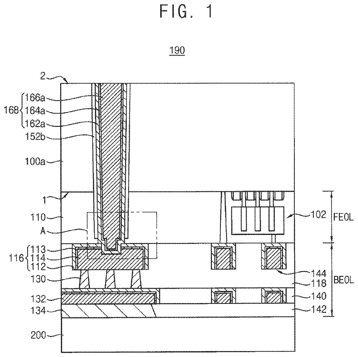
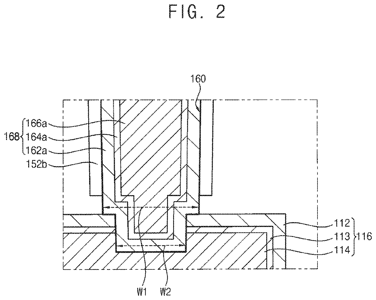
[0016]FIG. 1 is a cross-sectional view illustrating a semiconductor device 190 including a TSV in accordance with example embodiments. FIG. 2 is an enlarged cross-sectional view of a portion “A” in FIG. 1.

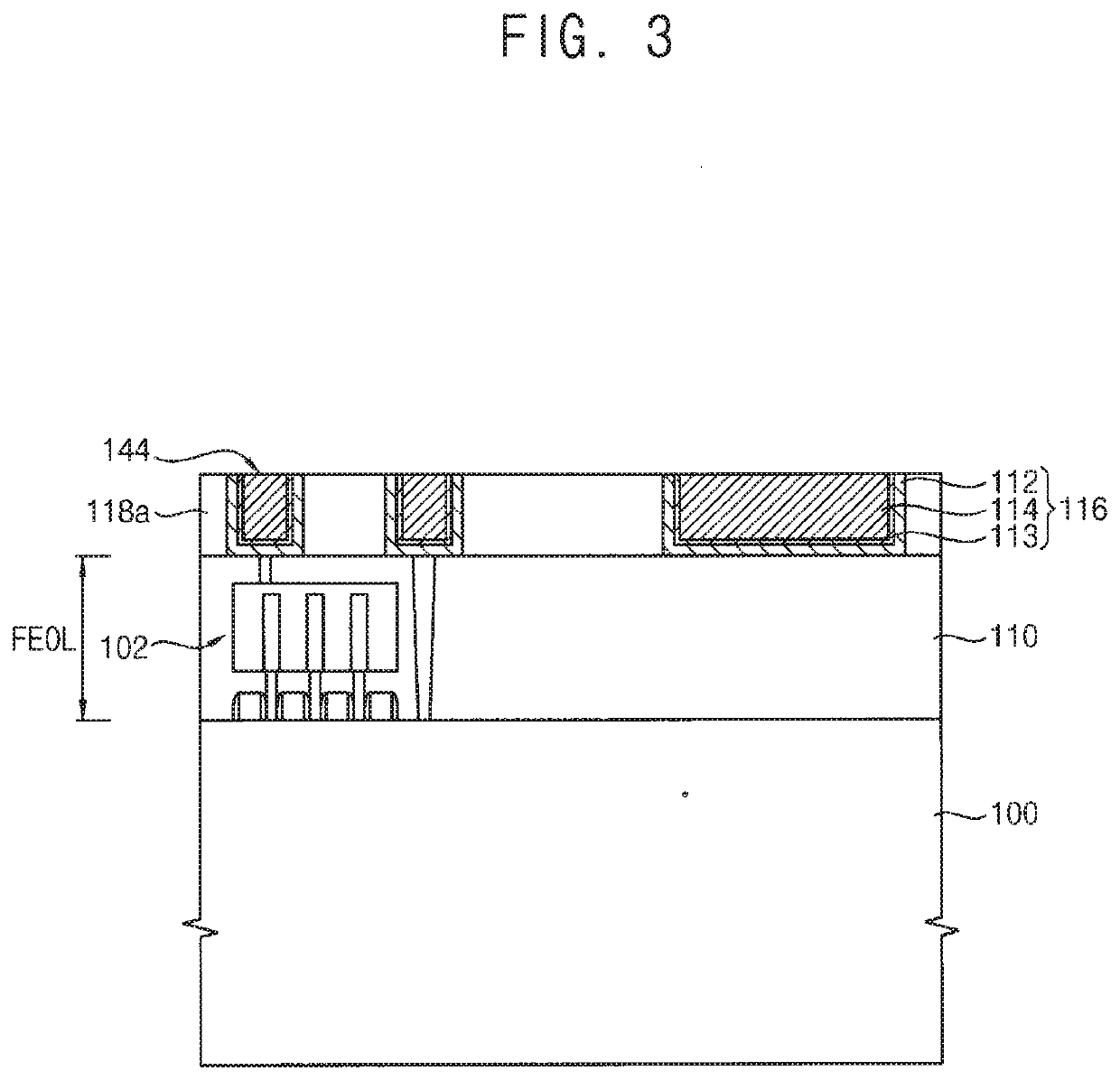
[0017]Referring to FIGS. 1 and 2, the semiconductor device 190 may include a substrate 100a, a first insulating interlayer 110, a pad pattern 116, and a through silicon via 168. In addition, the semiconductor device 190 may further include an insulation liner 152b, circuit elements 102, a first wiring structure 144, a second wiring structure 132, a pad electrode 134, a second insulating interlayer 118, a third insulating interlayer 140 and a fourth insulating interlayer 142.

[0018]The substrate 100a may include a semiconductor material. The substrate 100a may include, e.g., a silicon substrate, a germanium substrate, a silicon-germanium substrate, a silicon-on-insulator (SOI) substrate, a germanium-on-insulator (GOI) substrate, etc. In example embodiments, the substrate 100a may be ...


PUM

PropertyMeasurementUnit
temperatureaaaaaaaaaa
aspect ratioaaaaaaaaaa
insulatingaaaaaaaaaa

Abstract

A semiconductor device is provided. The semiconductor device includes a first insulating interlayer disposed on a first surface of a substrate; a pad pattern disposed on a lower surface of the first insulating interlayer, the pad pattern including a first copper pattern; and a through silicon via passing through the substrate and the first insulating interlayer, and contacting the first copper pattern of the pad pattern. The through silicon via includes a first portion passing through the substrate and the first insulating interlayer, and a second portion under the first portion and extending to a portion of the first copper pattern in the pad pattern. A boundary of the through silicon via has a bent portion between the first portion and the second portion.

Description

CROSS-REFERENCE TO THE RELATED APPLICATION[0001]This application claims priority from Korean Patent Application No. 10-2018-0135569, filed on Nov. 7, 2018 in the Korean Intellectual Property Office, the disclosure of which is incorporated by reference herein in its entirety.BACKGROUND1. Field[0002]Apparatuses and methods consistent with example embodiments relate to a semiconductor device and method of manufacturing the same. More particularly, example embodiments relate to a semiconductor device including a through silicon via (TSV) formed through a silicon substrate and connected with a pad and methods of manufacturing the same.2. Related Art[0003]In a multi-chip package, stacked semiconductor chips may be electrically connected with each other using, e.g., a conductive bump. In this case, a through silicon via electrically connecting the conductive bump to a pad of the semiconductor chip may be formed in a semiconductor device.[0004]Additionally, a via hole may be formed through ...

Claims


Application Information

Patent Timeline
Patent Type & Authority Applications(United States)
IPC IPC(8): H01L23/48H01L21/768H01L23/31
CPCH01L21/76898H01L23/481H01L21/76805H01L23/3128H01L21/76873H01L21/76831H01L23/485H01L23/528H01L21/76877H01L2924/181H01L2224/16225H01L2224/16245H01L2924/15311H01L21/76814H01L21/6835H01L2221/6834H01L2221/68327H01L2924/00012H01L23/49827H01L23/5226H01L23/5384H01L21/28194H01L27/14636H01L21/76829H01L21/76834H01L21/76807H01L21/76871H01L21/76844
Inventor SEO, JU-BINPARK, SU-JEONGKIM, TAE-SEONGMOON, KWANG-JINLIM, DONG-CHANCHOI, JU-IL
Owner SAMSUNG ELECTRONICS CO LTD
Why Eureka
Try Eureka