

Electronic Device Including a Contact Structure Contacting a Layer
Active Publication Date: 2020-05-07
SEMICON COMPONENTS IND LLC
View PDF0 Cites 0 Cited by
- Summary
- Abstract
- Description
- Claims
- Application Information
AI Technical Summary
Benefits of technology
The patent text is describing a cross-sectional view of a portion of a workpiece including a semiconductor layer, an insulating layer, and a contact opening extending through the insulating layer. The technical effect of the patent is to provide information on the structure of a portion of a semiconductor device in order to better understand its performance and reliability.
Problems solved by technology
On-state resistance between a source and drain within a power transistor can result in power loss within the transistor.
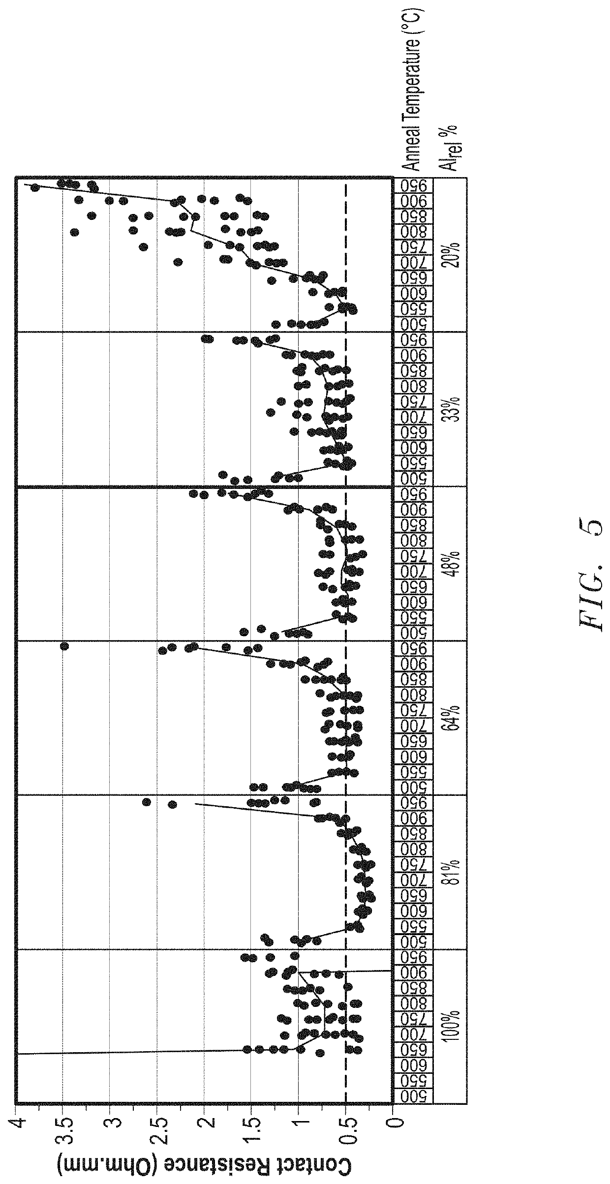
Even with all of the selections of the film order, composition, and thicknesses, the contact resistance may still not be low enough.
Method used
View moreImage
Smart ImageViewing Examples

Examples
embodiment 1
[0114]An electronic device can include a semiconductor layer and
[0115]a contact structure forming an ohmic contact with the semiconductor layer. The contact structure can include a first phase and a second phase different from the first phase, wherein the first phase includes Al, the second phase includes the metal, and the first phase contacts the semiconductor layer.
embodiment 2
[0116]The electronic device of Embodiment 1, wherein an interface between the semiconductor layer and the contact structure is free of an oxide.
embodiment 3
[0117]The electronic device of Embodiment 1, wherein the second phase includes Al3Me, Me2AlN, MeN, or a combination thereof, wherein Me is the metal.
Login to View More PUM
 Abstract
An electronic device can include a semiconductor layer and a contact structure forming an ohmic contact with the layer. In an embodiment, the semiconductor layer can include a III-N material, and the contact structure includes a first phase and a second phase, wherein the first phase includes Al, the second phase includes a metal, and the first phase contacts the semiconductor layer. In another embodiment, the semiconductor layer can be a monocrystalline layer having a surface along a crystal plane. The contact structure can include a polycrystalline material including crystals having surfaces that contact the surface of the monocrystalline layer, wherein a lattice mismatch between the surface of the monocrystalline layer and the surfaces of the crystals is at most 20%.
Description
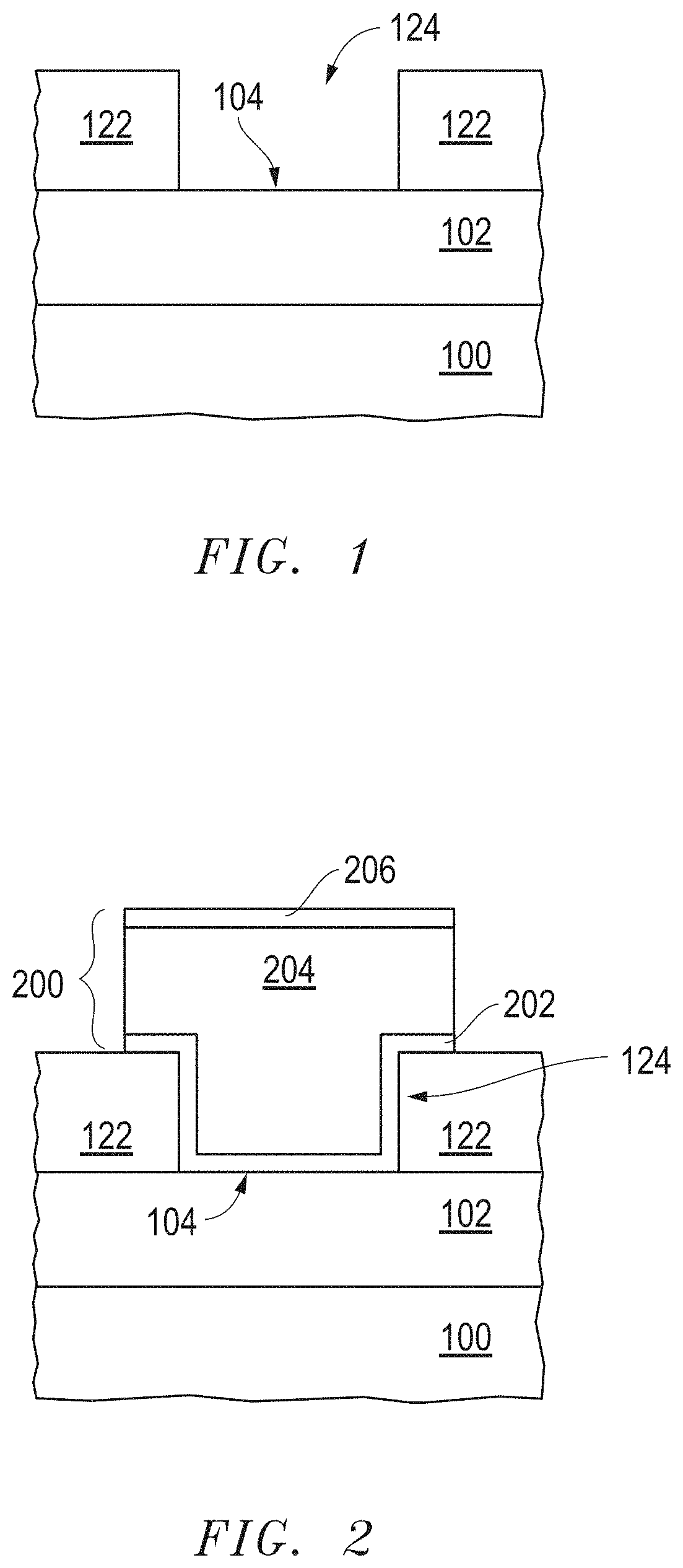
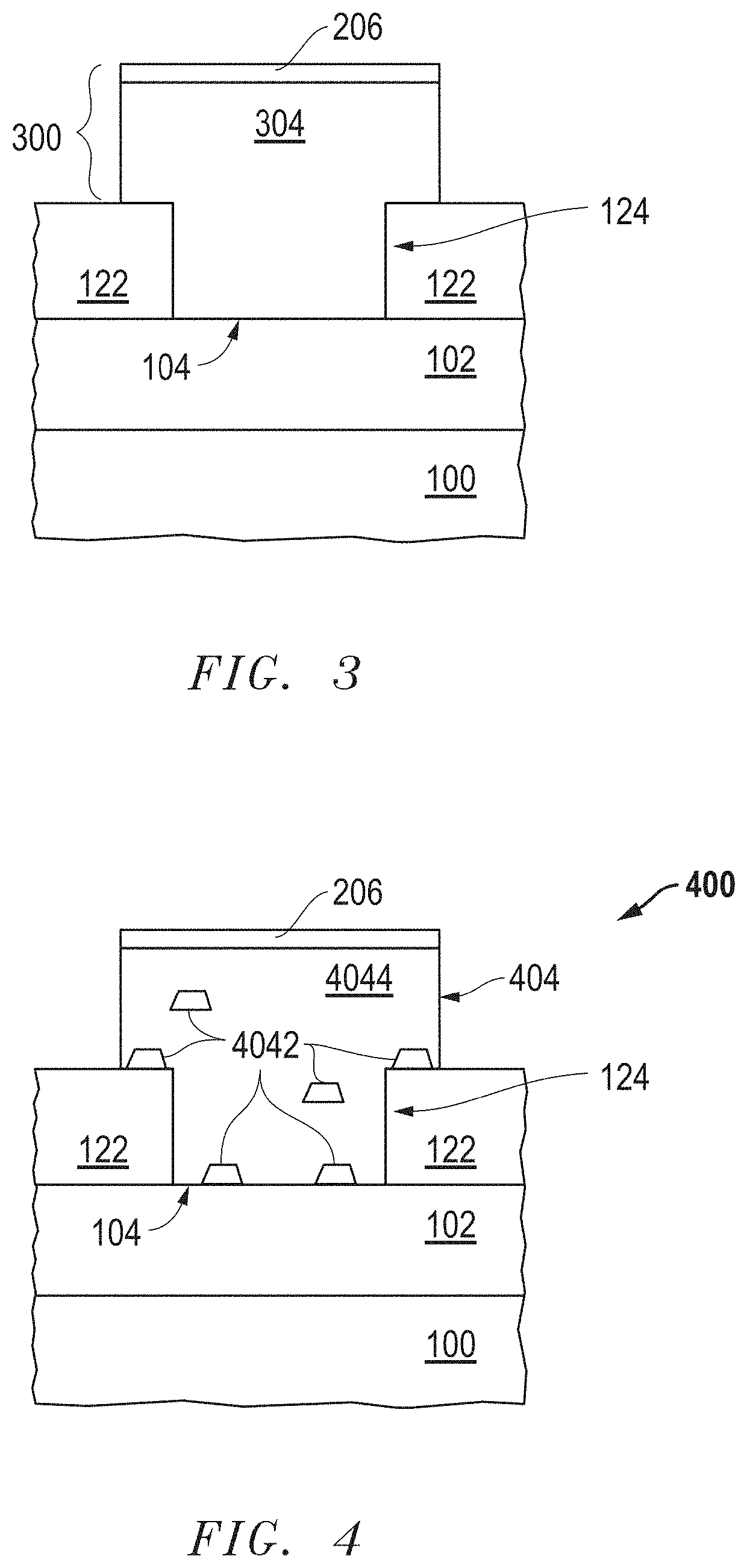
FIELD OF THE DISCLOSURE[0001]The present disclosure relates to electronic devices and processes of forming electronic devices, and more particularly to, electronic devices including contact structures contacting layers and processes of forming the same.RELATED ART[0002]A power transistor has relatively large current flowing through the active region of the transistor when the transistor is in the on-state. On-state resistance between a source and drain within a power transistor can result in power loss within the transistor. Contact resistance between a conductive structure (e.g., a source or drain electrode) and an underlying layer is part of the on-state resistance, and thus, lower contact resistance results in less power loss within the transistor. Many contact structures can include a bulk conductive film, such as an Al alloy, with at least one other film above or below the bulk conductive film. Such other film may be an adhesion film, a diffusion barrier film, an anti-reflectiv...
Claims
Login to View More Application Information
Patent Timeline
 IPC IPC(8): H01L23/532H01L21/02H01L21/04H01L21/786
CPCH01L21/28575H01L2224/05166H01L2224/05124H01L21/786H01L23/53214H01L21/76886H01L21/02057H01L29/452H01L2224/05181H01L23/53219H01L2224/0517H01L21/0485H01L29/2003H01L29/778H01L29/045H01L29/1066H01L29/7786
InventorCONSTANT, AURORECOPPENS, PETERBAELE, JORIS
OwnerSEMICON COMPONENTS IND LLC