Method for direct bonding two silicon wafers for minimising interfacial oxide and stresses at the bond interface, and an SOI structure

a technology of interfacial oxide and stress at the bond interface, which is applied in the direction of basic electric elements, semiconductor/solid-state device manufacturing, electric apparatus, etc., can solve the problems of reducing the operating efficiency of semiconductor bipolar devices subsequently formed, preparing a semiconductor substrate, and high production costs

Inactive Publication Date: 2004-05-06
ANALOG DEVICES INC
View PDF1 Cites 52 Cited by
  • Summary
  • Abstract
  • Description
  • Claims
  • Application Information

AI Technical Summary

Problems solved by technology

The layers must be relatively thick epitaxial silicon layers and are thus relatively expensive to produce, and may suffer from inherent defects.
Additionally, the deposition of epitaxial layers requires thermal cycles for the deposition, and it has been found that such thermal cycles can result in the formation of oxide layers, which reduce the operating efficiency of semiconductor bipolar devices subsequently formed.
However, two problems arise in the preparation of a semiconductor substrate from two directly bonded silicon wafers.
Firstly, it is virtually impossible to prevent the formation of an interfacial oxide layer at the bond interface.
Such an oxide layer or oxide islands at the bond interface causes many problems.
Additionally, the presence of an interfacial oxide layer or interfacial oxide islands at a bond interface of such a semiconductor substrate formed from two wafers may render the semiconductor substrate virtually unusable in connection with micro-mechanical or micro-electromechanical components.
In general, the presence of interfacial oxide along the bond interface of such a semiconductor substrate can lead to subsequent deformation and / or fracturing or other such failure of the micro-mechanical or micro-electromechanical component in the semiconductor substrate.
Secondly, in practice it has been found virtually impossible to directly bond a pair of silicon wafers together without interfacial stresses being induced in the silicon / silicon bond interface between the bonded wafers forming the semiconductor substrate.
However, in practice it has been found virtually impossible to accurately align the wafers so that the facial atoms at the bond faces of the respective wafers are accurately aligned at the bond interface.
Mechanical and optical alignment systems do not permit alignment of the wafers with the degree of accuracy required in order to align the wafers with their respective facial atoms aligned with each other.
Thus, in general, the facial atoms at the silicon / silicon bond interface of such bonded wafers are seldom if ever accurately aligned, and if accurately aligned, in general, are aligned by accident only.
It has been found that when misaligned, stresses build up between the facial atoms at the bond interface, thus leading to interfacial stresses at the bond interface.
For example, electrical resistance at the silicon / silicon bond interface increases with interfacial stress, and furthermore, interfacial stresses can lead to bowing and even fracturing of micro-mechanical components, for example, micro-mirrors, where such components are fabricated in the semiconductor substrate formed by such bonded wafers.
Additionally, interfacial stresses induced in the bond interface between directly bonded wafers of such semiconductor substrates cause crystal dislocations in the silicon at and near the bond interface.
Both of these effects degrade the performance of electronic devices formed in such semiconductor substrates.

Method used


Image

  • Method for direct bonding two silicon wafers for minimising interfacial oxide and stresses at the bond interface, and an SOI structure
  • Method for direct bonding two silicon wafers for minimising interfacial oxide and stresses at the bond interface, and an SOI structure
  • Method for direct bonding two silicon wafers for minimising interfacial oxide and stresses at the bond interface, and an SOI structure

Examples


Embodiment Construction

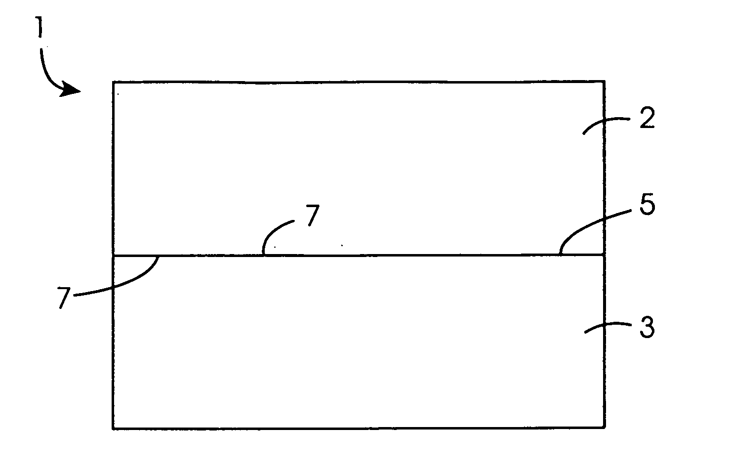
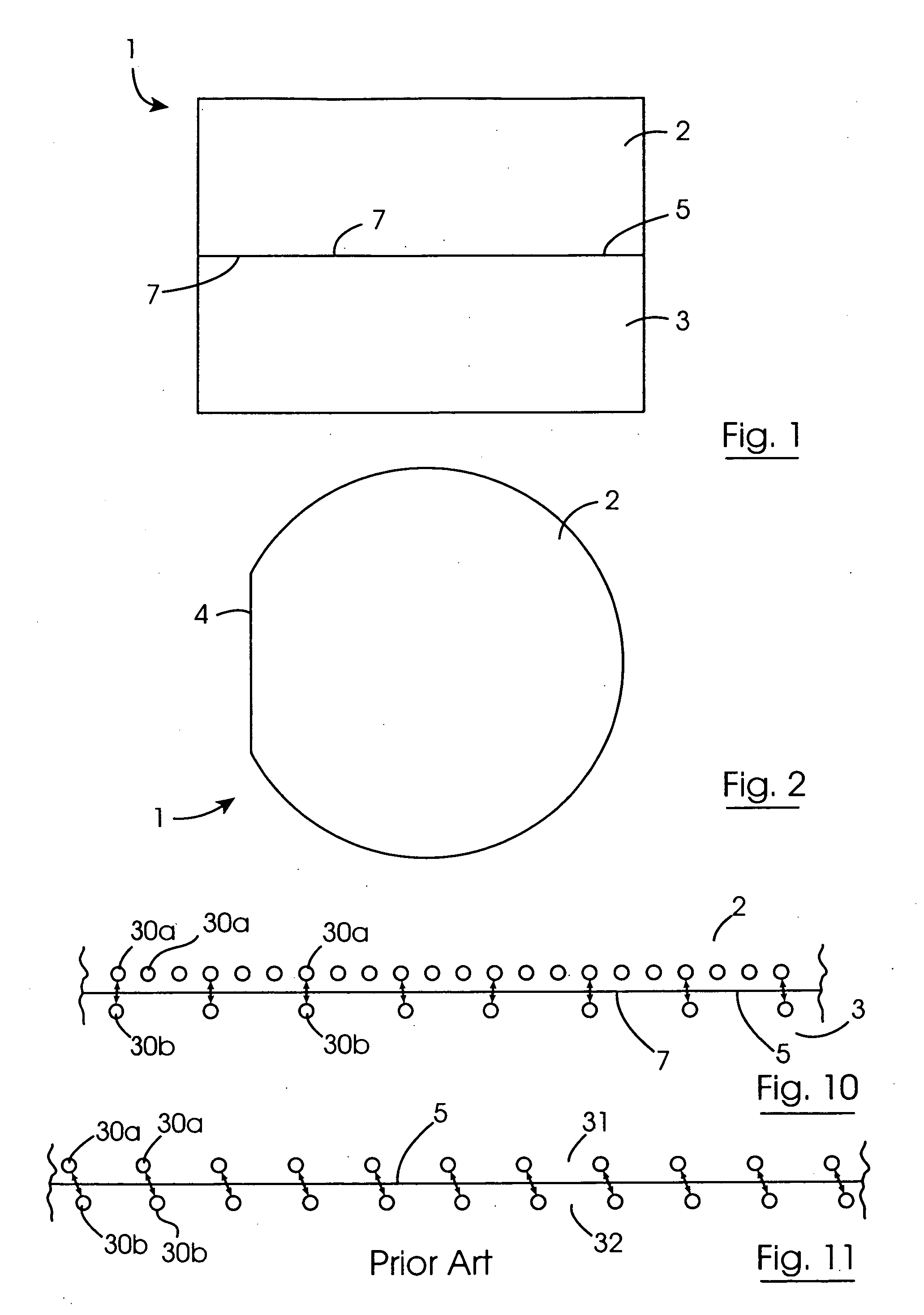
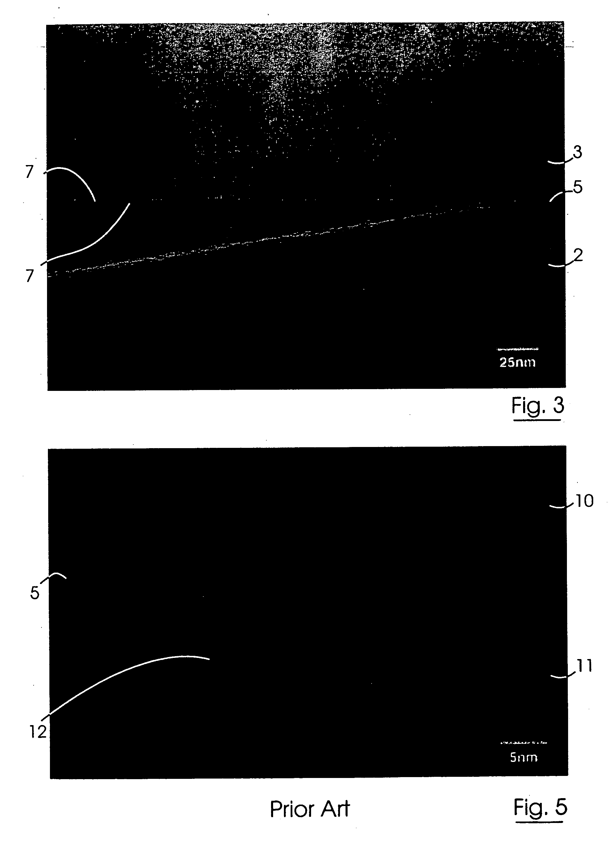
[0100] Referring to the drawings and initially to FIGS. 1 and 2, there is illustrated a semiconductor substrate according to the invention, indicated generally by the reference numeral 1. The substrate 1 comprises a pair of silicon wafers, namely, a first wafer 2 and a second wafer 3 both of single crystal silicon, which are bonded directly together along a silicon / silicon bond interface 5, along which interfacial oxide and interfacial stresses are minimised. By minimising interfacial stresses along the bond interface 5, crystal dislocations at and near the bond interface 5, which would otherwise result from such interfacial stresses are minimised and effectively eliminated. The substrate 1 is particularly suitable for forming electronic components, for example, bipolar devices, PIN diodes and insulated gate bipolar transistors, and indeed, any other electronic components which require two silicon layers of respective different electrical characteristics, and in particular, two laye...


PUM


Abstract

A semiconductor substrate (1) comprises first and second silicon wafers (2,3) directly bonded together with interfacial oxide and interfacial stresses minimised along a bond interface (5), which is defined by bond faces (7) of the first and second wafers (2,3). Interfacial oxide is minimised by selecting the first and second wafers (2,3) to be of relatively low oxygen content, well below the limit of solid solubility of oxygen in the wafers. In order to minimise interfacial stresses, the first and second wafers are selected to have respective different crystal plane orientations. The bond faces (7) of the first and second wafers (2,3) are polished and cleaned, and are subsequently dried in a nitrogen atmosphere. Immediately upon being dried, the bond faces (7) of the first and second wafers (2,3) are abutted together and the wafers (2,3) are subjected to a preliminary anneal at a temperature of at least 400° C. for a time period of a few hours. As soon as possible after the preliminary anneal, and preferably, within forty-eight hours of the preliminary anneal, the first and second wafers (2,3) are fusion bonded at a bond anneal temperature of approximately 1,150° C. for a time period of approximately three hours. The preliminary anneal may be omitted if fusion bonding at the bond anneal temperature is carried out within approximately six hours of the wafers (2,3) being abutted together. An SOI structure (50) may subsequently be prepared from the semiconductor structure (1) which forms a substrate layer (52) supported on a handle layer (55) with a buried insulating layer (57) between the substrate layer (52) and the handle layer (55).

Description

[0001] The present invention relates to a method for direct bonding two silicon wafers together for minimising interfacial oxide and interfacial stresses at the silicon / silicon bond interface. The invention also relates to a semiconductor substrate formed with two wafers bonded together with interfacial oxide and stresses minimised at the silicon / silicon bond interface. Further, the invention relates to a semiconductor on insulator structure, and to a method for preparing the semiconductor on insulator structure.BACKGROUND TO THE INVENTION[0002] Semiconductor substrates comprising two silicon wafers directly bonded to define a silicon / silicon bond interface have many uses, for example, integrated circuits may be fabricated in such substrates, and such integrated circuits may include CMOS and / or bipolar devices, PIN diodes, insulated gate bipolar transistors, and the like. Additionally, micro-mechanical components, such as micro-mirrors, as well as micro-electromechanical components ...

Claims


Application Information

Patent Timeline
Patent Type & Authority Applications(United States)
IPC IPC(8): H01L21/18H01L21/762
CPCH01L21/76251H01L21/187
Inventor MCCANN, PAUL DAMIENNEVIN, WILLIAM ANDREW
Owner ANALOG DEVICES INC
Why Eureka
Try Eureka