
Multilayer ceramic capacitor

a ceramic capacitor and multi-layer technology, applied in the direction of fixed capacitors, stacked capacitors, fixed capacitor details, etc., can solve the problems of short circuit, low insulation, deformation of reliability, etc., and achieve the effects of suppressing the deterioration of the smoothness of the dielectric layer, small thickness variation, and reducing the starting temperature of grain growth

Active Publication Date: 2020-06-11
MURATA MFG CO LTD
View PDF0 Cites 3 Cited by
  • Summary
  • Abstract
  • Description
  • Claims
  • Application Information

AI Technical Summary

Benefits of technology

The present invention provides a multilayer ceramic capacitor with reduced short-circuit rate, large electrostatic capacity, and improved mean time to failure (MTTF) while including thin dielectric layers. The ceramic crystal grains have Si on their surfaces, which causes the grains to slide and form thin and thick portions in the dielectric layers. The Mg content of the dielectric layers can be reduced to lower the grain growth starting temperature and prevent the formation of balls from the metal contained in the inner electrode layers. The crystal grains are also less likely to slide on the crystal grain surfaces, inhibiting plastic deformation. The small thickness variation of the dielectric layers prevents deterioration in smoothness and ensures a smooth capacitor performance.

Problems solved by technology

Although there is a demand for compact multilayer ceramic capacitors, a multilayer ceramic capacitor including thin dielectric layers and thin inner electrode layers has an issue where formation of partially thin dielectric layers during grain growth causes short circuits and low insulation and degrades reliability.

Method used


Image

  • Multilayer ceramic capacitor
  • Multilayer ceramic capacitor
  • Multilayer ceramic capacitor

Examples


experimental examples

3. Experimental Examples

(1) Experimental Example 1

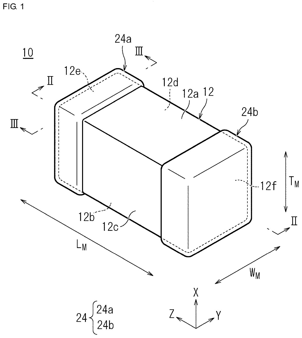
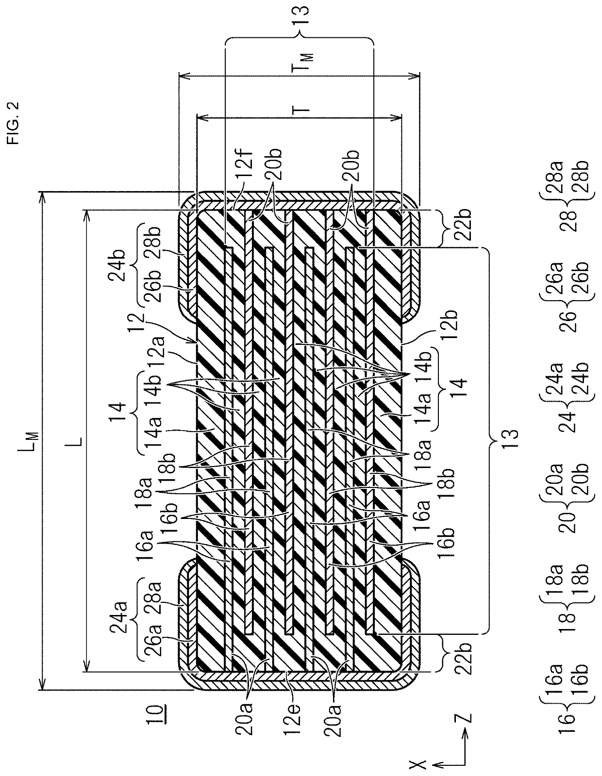
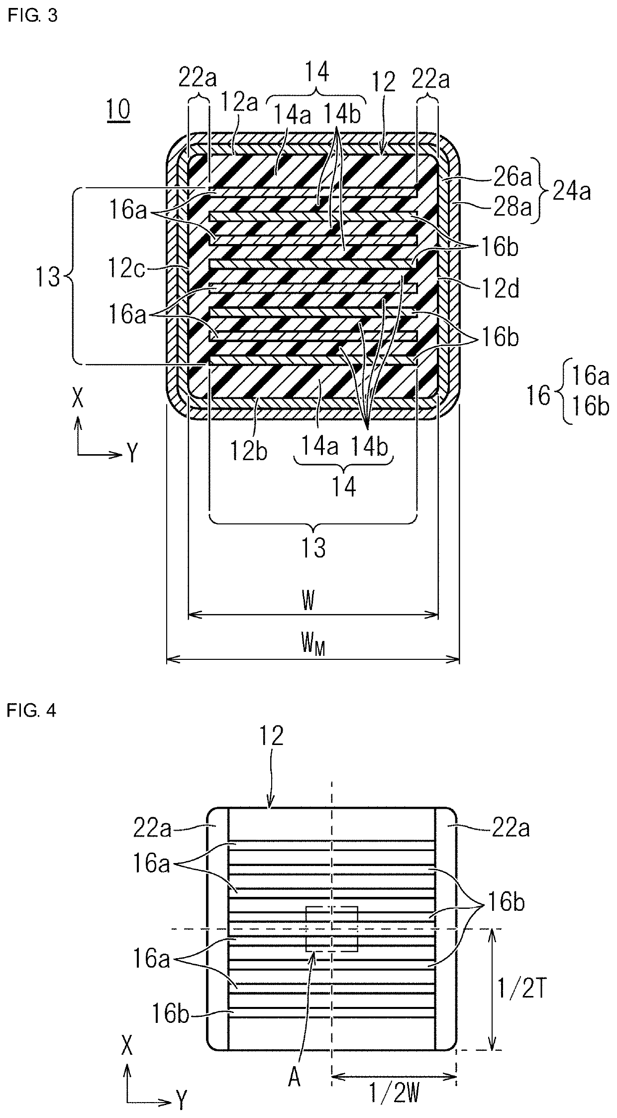
[0063]A multilayer ceramic capacitor 10 was produced according to the above method for manufacturing a multilayer ceramic capacitor, and individual multilayer chips during manufacture were checked for their stacked state. In this case, W gap sections 22a were formed by attaching a dielectric having the same composition as the dielectric layers in the effective section 13. For sample number 1-38, a heat treatment was performed at a maximum temperature of 1085° C. for 35 minutes. The obtained dielectric raw material mixture was subjected to ICP emission spectrometry, and it was found that the composition of the dielectric raw material mixture was substantially the same as the preparation composition shown in Table 1.

[0064]The specification of the multilayer ceramic capacitor 10 used in Experimental Example 1 was as follows: the dimension L in the longitudinal direction z from the first end surface 12e to the second end surface 12f was ...


PUM

PropertyMeasurementUnit
molar ratioaaaaaaaaaa
thicknessaaaaaaaaaa
thicknessaaaaaaaaaa

Abstract

A multilayer ceramic capacitor that includes outer electrodes and a multilayer body having stacked inner electrode layers and dielectric layers. The dielectric layers in an effective section contain, relative to 100 parts by mole of Ti, 0.7 to 1.2 parts by mole of Si, 0.9 to 1.1 parts by mole of Dy, 0.24 to 0.34 parts by mole of Mg, 0.17 to 0.23 parts by mole of Al, 0.09 to 0.11 parts by mole of Mn, and 0.04 to 0.06 parts by mole of V. The dielectric layers have a Ba / Ti molar ratio of 1.0073 to 1.0083.

Description

CROSS REFERENCE TO RELATED APPLICATIONS[0001]The present application claims priority to Japanese Patent Application No. 2018-229818, filed Dec. 7, 2018, the entire contents of which is incorporated herein by reference.BACKGROUND OF THE INVENTION1. Field of the Invention[0002]The present invention relates to a multilayer ceramic capacitor.2. Description of the Related Art[0003]In recent years, there has been a demand for compact multilayer ceramic capacitors having large electrostatic capacity. The requirements for multilayer ceramic capacitors are increasing year by year.[0004]One of methods for forming dielectric layers with high permittivity in a multilayer ceramic capacitor is a method for growing ceramic grains (crystal grains) (Japanese Unexamined Patent Application Publication No. 2014-210685).SUMMARY OF THE INVENTION[0005]Although there is a demand for compact multilayer ceramic capacitors, a multilayer ceramic capacitor including thin dielectric layers and thin inner electro...

Claims


Application Information

Patent Timeline
Patent Type & Authority Applications(United States)
IPC IPC(8): H01G4/12H01G4/30H01G4/012H01G4/232H01G4/248
CPCH01G4/248H01G4/1227H01G4/232H01G4/012H01G4/30H01G4/1209C04B35/4682
Inventor UCHIDA, KAZUHISAMURANISHI, NAOTO
Owner MURATA MFG CO LTD
Learn More