
Eureka
For R&D, Eureka makes reading and utilizing patents & technical documents easy.
Eureka AIR
Designed for self-driven R&D workflows. Generate viable solutions, solve complex R&D challenges, empower your innovation with AI.

Eureka Materials
Designed for material experts only. Revolutionize your material R&D, from search, analyze, to developing new materials.

TechResearch
Generate reliable direction feasibility study reports for your R&D in just a few steps.

TechSeek
Discover and master advanced knowledge NOW. Basics, ideas, possibilities, all at once.

TechMind
As an expert in R&D Theories, TechMind can generates customized viable solutions instantly.

TechRisk
Analyze your overall solution with one click, know your potential R&D risks in advance.

TechMonitor
Get weekly tech updates, stay abreast of the latest tech innovations and key insights.
Display module and electronic device
- Summary
- Abstract
- Description
- Claims
- Application Information
AI Technical Summary
Benefits of technology
Problems solved by technology
Method used
Image

Examples
first embodiment
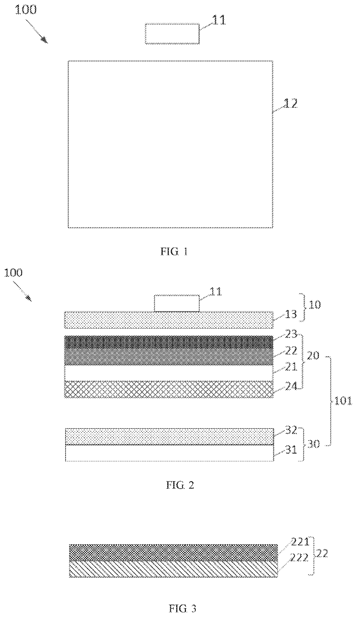
[0026]Referring to FIGS. 2-3, FIG. 2 is a schematic structural view of a display module according to the present invention.
[0027]As shown in FIG. 2, the display module of the present invention includes a backlight module 10 and a liquid crystal display panel 101.
[0028]The backlight module 10 includes a light source 11 and may further include a light guide plate 13. The light guide plate 13 is located above the light source 11.
[0029]The liquid crystal display panel includes an array substrate 20 and a color filter substrate 30, wherein the array substrate 20 is provided with a blue filter film 23 on a side close to the light source 11. The blue filter film 23 is disposed between the light guide plate 13 and a top of the array substrate 20.
[0030]The array substrate 20 includes a glass substrate 21, a switch array layer 24, a polarizer 22, and a blue filter film 23. The switch array layer 24 is disposed on a second surface (lower surface) of the glass substrate 21, and the polarizer 2...
second embodiment
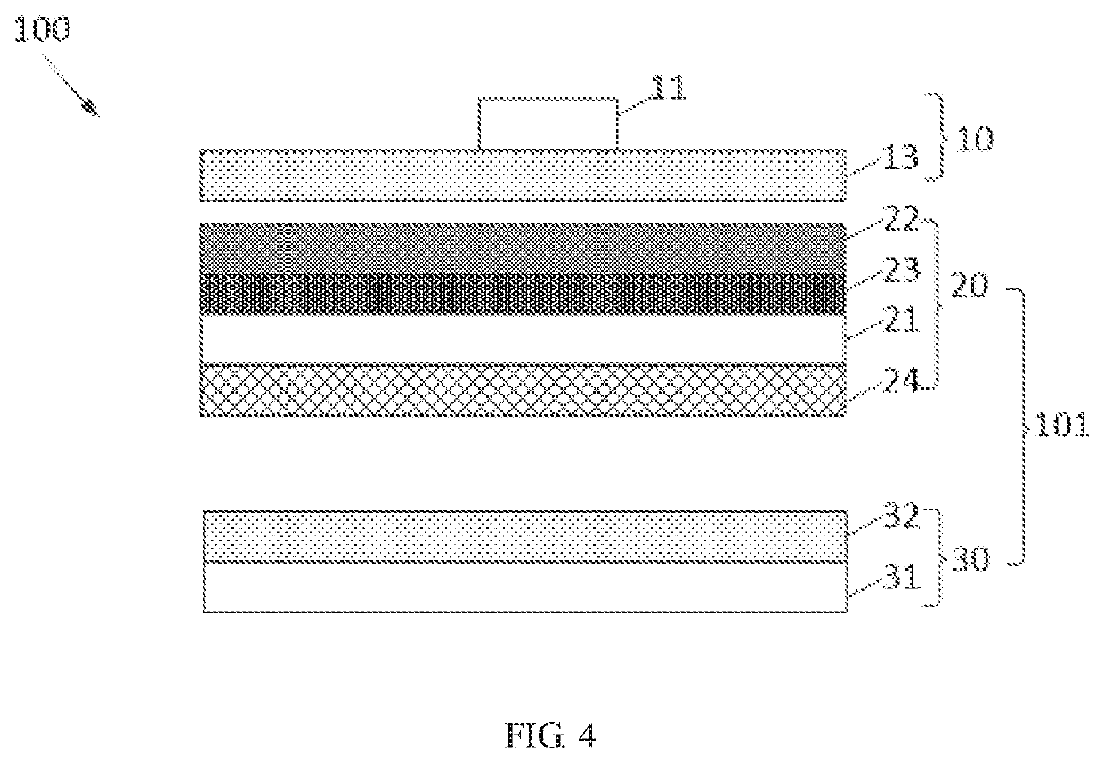
[0038]Referring to FIG. 4, FIG. 4 is a schematic structural view of a display module according to the present invention.
[0039]As shown in FIG. 4, the display module of the present invention includes a backlight module 10 and a liquid crystal display panel 101.
[0040]The backlight module 10 includes a light source 11 and may further include a light guide plate 13. The light guide plate 13 is disposed above the light source 11.
[0041]The liquid crystal display panel includes an array substrate 20 and a color filter substrate 30, wherein the array substrate 20 is provided with a blue filter film 23 on a side close to the light source 11.
[0042]The array substrate 20 includes a base substrate, a polarizer 22 and a blue filter film 23. The substrate includes a glass substrate 21 and a switch array layer 24. The switch array layer 24 is disposed on a second surface (lower surface) of the glass substrate 21, and the polarizer 22 is disposed on a first surface (upper surface) of the glass sub...
PUM
 Abstract
Description
Claims
Application Information
 - R&D Engineer
- R&D Manager
- IP Professional
- Industry Leading Data Capabilities
- Powerful AI technology
- Patent DNA Extraction
Browse by: Latest US Patents, China's latest patents, Technical Efficacy Thesaurus, Application Domain, Technology Topic, Popular Technical Reports.
© 2024 PatSnap. All rights reserved.Legal|Privacy policy|Modern Slavery Act Transparency Statement|Sitemap|About US| Contact US: help@patsnap.com