Semiconductor manufacturing device

a manufacturing device and semiconductor technology, applied in the direction of conveyor parts, transportation and packaging, electric devices, etc., can solve the problems of operator suffocation, wafer loss, and increase the manufacturing cost of a semiconductor device, so as to improve the environment of the semiconductor manufacturing process, reduce the cost of semiconductor manufacturing, and reduce the cost

Inactive Publication Date: 2020-07-09
KIM SEONG LAE +2
View PDF0 Cites 5 Cited by
  • Summary
  • Abstract
  • Description
  • Claims
  • Application Information

AI Technical Summary

Benefits of technology

[0032]The present invention is characterized in that a load port unit, a substrate transfer unit and a process performing unit are sequentially provided along a transfer path of a semiconductor substrate and the dry purified air is circulated in place of the nitrogen gas in the load port unit and the substrate transfer unit, thereby being able to reduce the cost of semiconductor manufacturing by using dry purified air at a lower cost than nitrogen gas.
[0033]It is possible that the present invention, by circulating a dry purified air in place of nitrogen gas from FOUP, starting from the substrate transfer unit and then passing through the load port unit and FOUP sequentially, toward the substrate transfer unit, the dry purified air having the same dew point as nitrogen gas is used, can improve the environment of the semiconductor manufacturing process by minimizing the effect of moisture absorbed onto the semiconductor substrate, e.g. production of manufacturing process by-products or natural oxide films.
[0034]It is possible that the present invention, because the load port unit and the substrate transfer unit and the process performing unit are provided, and oxygen is included in the dry purified air while circulating the dry purified air instead of nitrogen gas, can have the same proportion of the oxygen and the nitrogen gas therein as the oxygen and the nitrogen in the atmosphere when the FOUP and the load port unit are attached/de

Problems solved by technology

However, when the semiconductor manufacturing device uses nitrogen gas as an ambient gas in the FOUP and wafer transfer chamber, because the nitrogen gas is specially manufactured and ordered at an expensive cost, the semiconductor device is partially lost toward the outside of the semiconductor manufacturing device when the FOUP and the load port are detached/attached or when the FOUP and the wafer transfer chamber are detached/attached, thereby raising the manufacturing cost of a semiconductor device.
Furthermore, when the semiconductor manufacturing device accom

Method used


Image

  • Semiconductor manufacturing device
  • Semiconductor manufacturing device
  • Semiconductor manufacturing device

Examples


Embodiment Construction

[0044]Hereinafter, preferred embodiment(s) of the present invention will be described in detail with reference to the accompanying drawings so that an ordinary person skilled in the art can easily carry out the present invention.

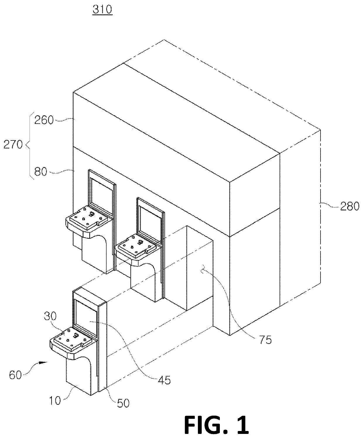
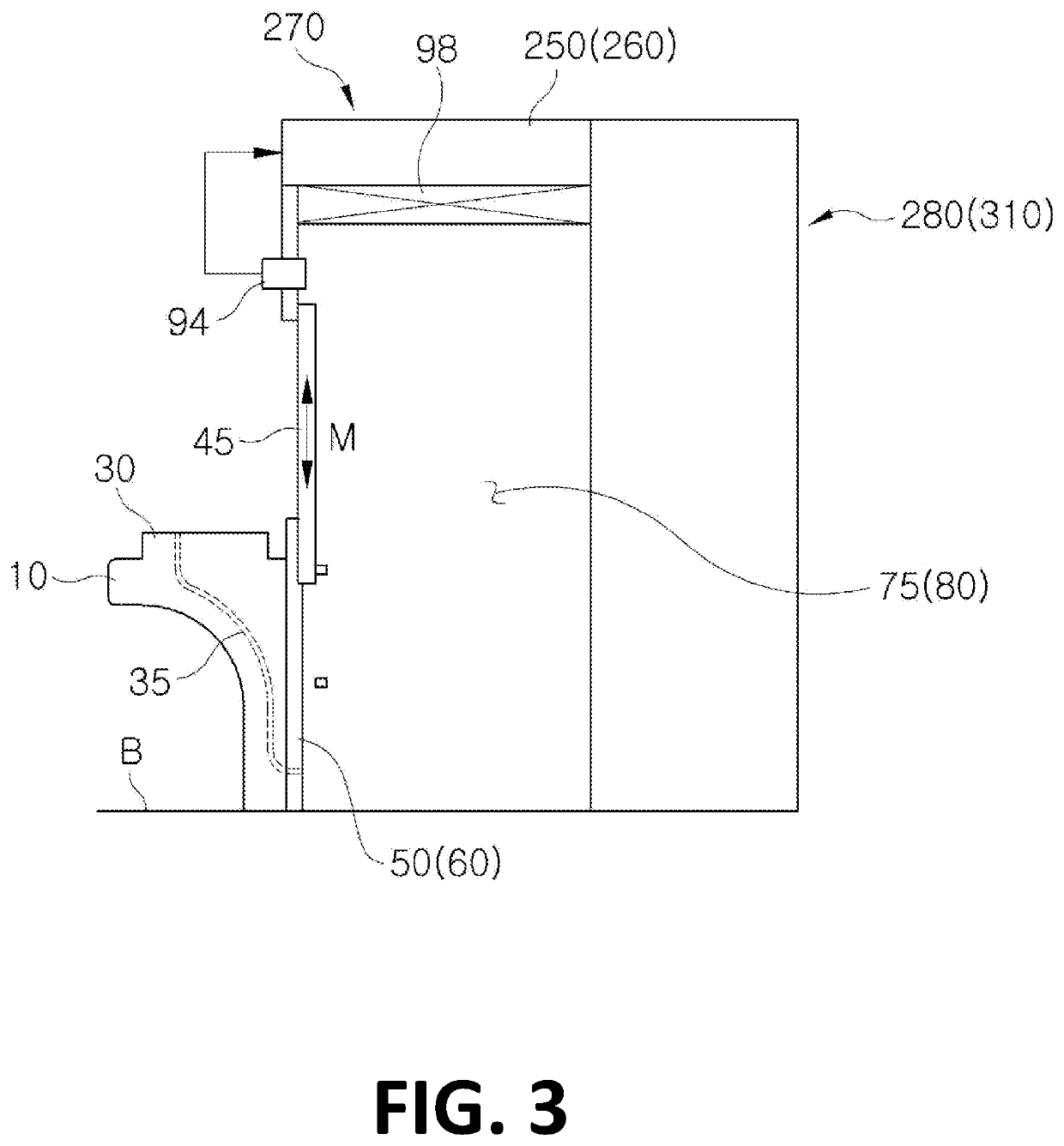
[0045]Referring to FIGS. 1 to 6, a semiconductor manufacturing device 310 according to the present invention includes a load port unit 60 sequentially arranged along a transfer path of a semiconductor substrate (W in FIG. 7), a substrate transfer unit 270 and a process performing unit 280. Herein, the load port unit 60 is received to the substrate transfer unit 270 while seating a FOUP 330 that receives a semiconductor substrate, as illustrated in FIG. 7.

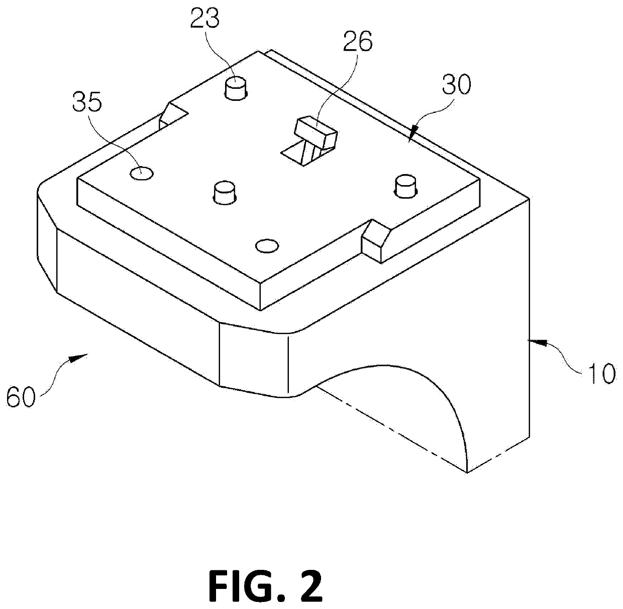
[0046]The load port unit 60 includes a load door 45 that is relatively movable with respect to the substrate transfer unit 270 and an air introduction flow paths (35 in FIG. 3) that connects the inside and the outside of the substrate transfer unit 270 under the load door 45. More specifically, the load port...


PUM


Abstract

A semiconductor manufacturing device, according to the present invention, comprises a load port unit, a substrate transfer unit, and a processing unit sequentially arranged along a transfer path of a semiconductor substrate, wherein the load port unit has a load door relatively movable with respect to the substrate transfer unit while being accommodated in the substrate transfer unit, and an air introduction path for connecting the inside and the outside of the substrate transfer unit under the load door; and the substrate transfer unit has a substrate processing module for communicating with the load port unit and the processing unit while limiting a processing space of the semiconductor substrate, and an air supply module positioned on the substrate processing module so as to supply dry, purified air to the substrate processing module.

Description

TECHNICAL FIELD[0001]The present invention relates to the semiconductor manufacturing device for protecting a semiconductor substrate of a FOUP by inflowing an ambient gas used in a transfer path of a semiconductor substrate during a semiconductor manufacturing process into a FOUP (Front Opening Unified Pod).BACKGROUND[0002]Generally, a semiconductor manufacturing factory has various kinds of semiconductor manufacturing devices. The semiconductor manufacturing device comprises, for function, a load port unit, a substrate transfer unit, and a process performing unit for performing a photo process, an etching process, or a deposition process, though there are some differences in external shape and internal structure depending on the unit process characteristics.[0003]Here, the load port unit is positioned in front of the substrate transfer unit to seat a FOUP that receives a semiconductor substrate. The substrate transfer unit separates the semiconductor substrate from the FOUP using ...

Claims


Application Information

Patent Timeline
IPC IPC(8): H01L21/677
CPCH01L21/67739H01L21/67775H01L21/67017H01L21/67772H01L21/67242
Inventor KIM, SEONG LAELIM, KWANGWOOK
Owner KIM SEONG LAE
Why Eureka
Try Eureka