
Measuring Thin Films on Grating and Bandgap on Grating

a technology of grating and thin film, applied in the direction of semiconductor/solid-state device testing/measurement, instruments, semiconductor devices, etc., can solve the problems of complex formation process of high-k metal gate film, insufficient x-ray, interfacial and crystalline defects

Active Publication Date: 2020-07-30
KLA CORP
View PDF2 Cites 1 Cited by
  • Summary
  • Abstract
  • Description
  • Claims
  • Application Information

AI Technical Summary

Benefits of technology

This approach significantly improves precision and reduces parameter correlation, enhancing measurement speed and robustness, enabling the accurate measurement of complex thin film stacks, including those with in-situ ALD processes, and meeting stringent semiconductor manufacturer specifications.

Problems solved by technology

The metal gate deposition can alter the materials properties and their composition through annealing or diffusion in addition to potentially causing interfacial and crystalline defects.
The high-k metal gate film formation process is complex.
X-ray metrology was used to measure the multi-layer stack on planar, but x-ray was insufficient because of the required precision 3 sigma (<0.04 A) and because of its insufficient sensitivity due to little scattering of the thin films.
But this method is not a satisfactory solution for at least three reasons.
First, the pre-layers process may not be stable enough to assign one fixed value for that parameter.
Third, throughput may be too slow for commercial manufacturing because multiple layers cannot be measured in one step.
Due to the loading effect where the deposition and etch rates are topography dependent, the 1D film data will not be in perfect correlation with the 2D or 3D ones.
Previous methods were used to perform these measurements, but both are either incapable of providing accurate measurements and / or too slow for commercial manufacturing.
This method cannot solve most of the issues and the requirements described above.
The all floating method also cannot deal with low contrast or thin materials.
This leads to correlation between concurrent parameters and, therefore, inaccurate measured film on grating thicknesses.
In an experiment, both simulation data and real experimental data obtained from the single AOI all floating method did not pass precision, accuracy, robustness, or wafer consistency tests.
While the single AOI all floating method can potentially meet the throughput and cost of ownership (COO) requirements, it failed in most technical checks.
For correlation, on the scale of zero to one when one represents a 100% parameter correlation, 0.958 and 0.846 correlations are considered high and represent a potential risk of the combined model and technique used.
The simulation showed poor precision results and high parameter correlation which do not meet the semiconductor manufacturer requirements for this layer.
Experimental data also showed results that are out of specification.
In the N Metal Gate (NMG) deposition layer, the film stack complexity increases at the late stage of the HKMG process.
The simulation data expects bad precision data and highly correlated parameters between all six film stacks.
Thus, the single AOI all floating method cannot provide accurate measurements of this layer.
However, this assumption is not valid for the current advanced technological nodes.
First, the DFF throughput is too slow for semiconductor manufacturers.
In other words, multiple layers need to be measured simultaneously, which is not possible with DFF.
Second, DFF cannot be used for the NMG (FIG. 4) layer and PMG layer.
DFF cannot be used with this particular process flow.
This assumption may be incorrect.
Fourth, any inaccuracy or error in pre-layer model is carried out to all post layers.
Fifth, any Library Boundary Hit (LBH) in an early pre-layer stage will interrupt all measurements in post layers.
Neither DFF nor the single AOI all floating method can provide solutions to the film on grating market due to one or more of inaccurate data out of specifications linearity to a reference method, poor precision and stability and matching, highly correlated critical and floating parameters, slow measurement (i.e., low throughput), high COO, inability to handle in-situ ALD process, high risk for LBH, and robustness test failures.

Method used


Image

  • Measuring Thin Films on Grating and Bandgap on Grating
  • Measuring Thin Films on Grating and Bandgap on Grating
  • Measuring Thin Films on Grating and Bandgap on Grating

Examples


example 1

[0140]In an example, the first effective medium dispersion model replaces five materials in a stack: IL, HK, TiN, TaN and TaL. By floating the first effective medium thickness and eventually the first effective medium Bruggeman effective medium approximation (BEMA) fraction, the first effective medium accounts for all process variation of the five layers together. Thus, the first scatterometry model floating parameters are reduced from the initial twelve parameters to only seven. Using first scatterometry model, the top TiN (8 A) film on grating was accurately measured and all success criteria were met including the robustness test. The top TiN (8 A) thickness was forwarded to another model.

[0141]The second effective medium dispersion model replaces four materials: IL, HK, TiN and TaN. By floating the second effective medium thickness and eventually the second effective medium BEMA fraction, the second effective medium accounts for all process variation of the four films together. T...

example 2

[0144]To validate the within layer feedforward technique in another example, three DOE wafers were designed and measured with the scanned AOI RPRC. Three sites per wafer were selected for the reference measurement TEM. FIG. 8 summarizes the FOG vs. TEM linearity results for TiN, TaL, and TaN using the SSDF method described in FIG. 6. In addition to the accuracy, the SDFF method was tested for precision GRR and robustness. Both R2 and Slope passed the customer requirement for linearity.

[0145]FIG. 9 shows the significance of the results of the SSDF method and compared with the old method of “all floating.” The GRR and robustness tests are more liable to being affected by the multiple films correlation. Both GRR and Robustness passed the customer specifications.

[0146]Successful FOG layers cases including some of the EM dispersion (measured using the Scanned AOI RPRC and used in the libraries) are presented below.

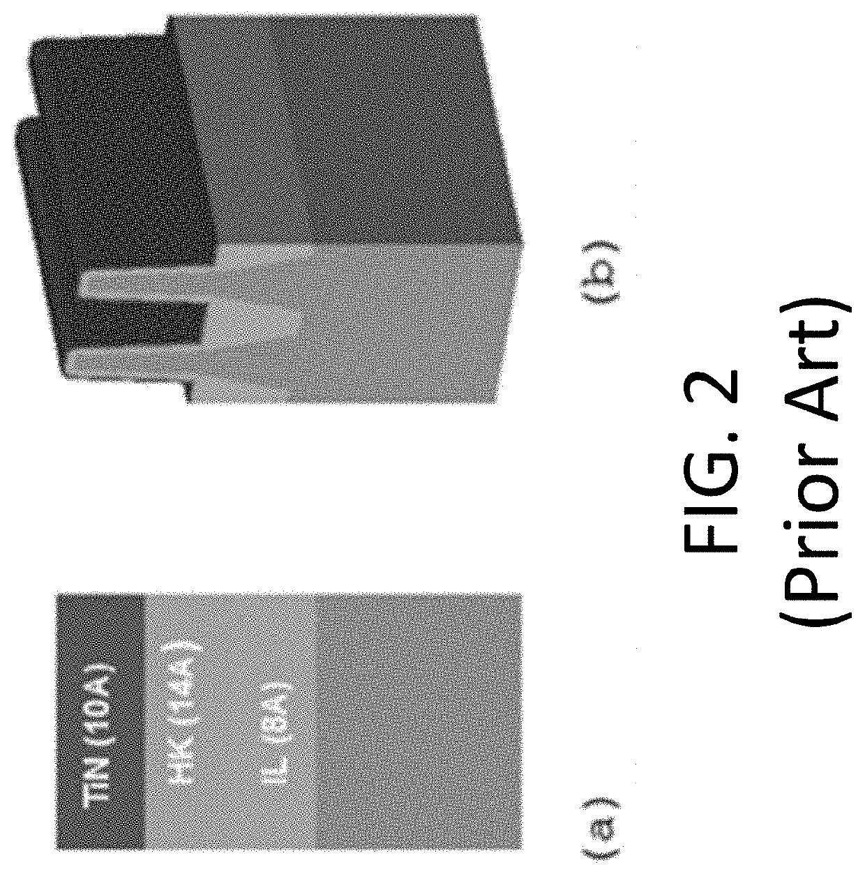
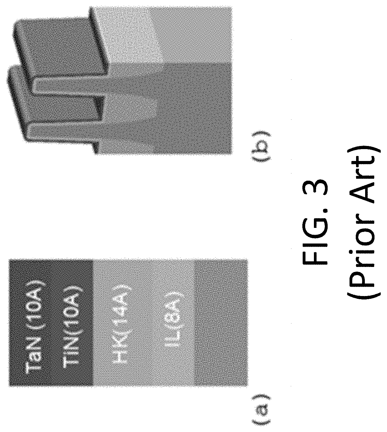
[0147]FIG. 2(a) shows the cap layer film stack and 2(b) shows the FOG cap ...


PUM

PropertyMeasurementUnit
sensitivityaaaaaaaaaa
wavelengthsaaaaaaaaaa

Abstract

Methods and systems disclosed herein can measure thin film stacks, such as film on grating and bandgap on grating in semiconductors. For example, the thin film stack may be a 1D film stack, a 2D film on grating, or a 3D film on grating. One or more effective medium dispersion models are created for the film stack. Each effective medium dispersion model can substitute for one or more layers. A thickness of one or more layers can be determined using the effective medium dispersion based scatterometry model. In an instance, three effective medium dispersion based scatterometry models are developed and used to determine thickness of three layers in a film stack.

Description

CROSS-REFERENCE TO RELATED APPLICATIONS[0001]This application is a continuation of U.S. application Ser. No. 15 / 800,877 filed Nov. 1, 2017, which claims priority to the provisional patent application filed Aug. 22, 2017 and assigned U.S. App. No. 62 / 548,579, the disclosures of which are hereby incorporated by reference.FIELD OF THE DISCLOSURE[0002]This disclosure relates to measuring thin films.BACKGROUND OF THE DISCLOSURE[0003]Evolution of the semiconductor manufacturing industry is placing ever greater demands on yield management and, in particular, on metrology and inspection systems. Critical dimensions are shrinking while wafer size is increasing. Economics is driving the industry to decrease the time for achieving high-yield, high-value production and better device performance. Thus, minimizing the total time from detecting a yield problem to fixing it determines the return-on-investment for the semiconductor manufacturer.[0004]To control device performance, in particular elec...

Claims


Application Information

Patent Timeline
Patent Type & Authority Applications(United States)
IPC IPC(8): G01B11/06G01B15/02H01L29/49H01L21/66
CPCH01L29/517H01L29/42364H01L29/42376G01B15/02H01L29/513H01L22/12H01L22/20H01L29/518H01L29/4966H01L29/66795G01B11/0625G01B11/06H01L21/02535H01L21/0254
Inventor CHOUAIB, HOUSSAMTAN, ZHENGQUAN
Owner KLA CORP
Features
  • Generate Ideas
  • Intellectual Property
  • Life Sciences
  • Materials
  • Tech Scout
  • Unparalleled Data Quality
  • Higher Quality Content
  • 60% Fewer Hallucinations
Learn More