
OLED display device and manufacturing method thereof

a technology of organic light-emitting diodes and display devices, which is applied in the field of displays, can solve the problems of reducing the lifespan of oled display devices, brittle materials, and polarizers having a thick thickness, and not being beneficial to the development of dynamic bending display panels

Active Publication Date: 2020-08-27
WUHAN CHINA STAR OPTOELECTRONICS SEMICON DISPLAY TECH CO LTD
View PDF9 Cites 1 Cited by
  • Summary
  • Abstract
  • Description
  • Claims
  • Application Information

AI Technical Summary

Benefits of technology

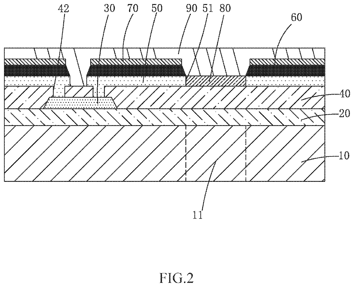
The present invention is an OLED display device with improved reflectivity and reduced cost. It includes a plurality of sub-pixels, a first insulating layer, a first metal layer, a second insulating layer, a second metal layer, a black matrix, a hard mask, and a plurality of color resists. The color resists are placed in openings that match the sub-pixels. This design effectively eliminates reflective light and reduces the number of masks required for manufacturing, resulting in a lower cost for OLED displays.

Problems solved by technology

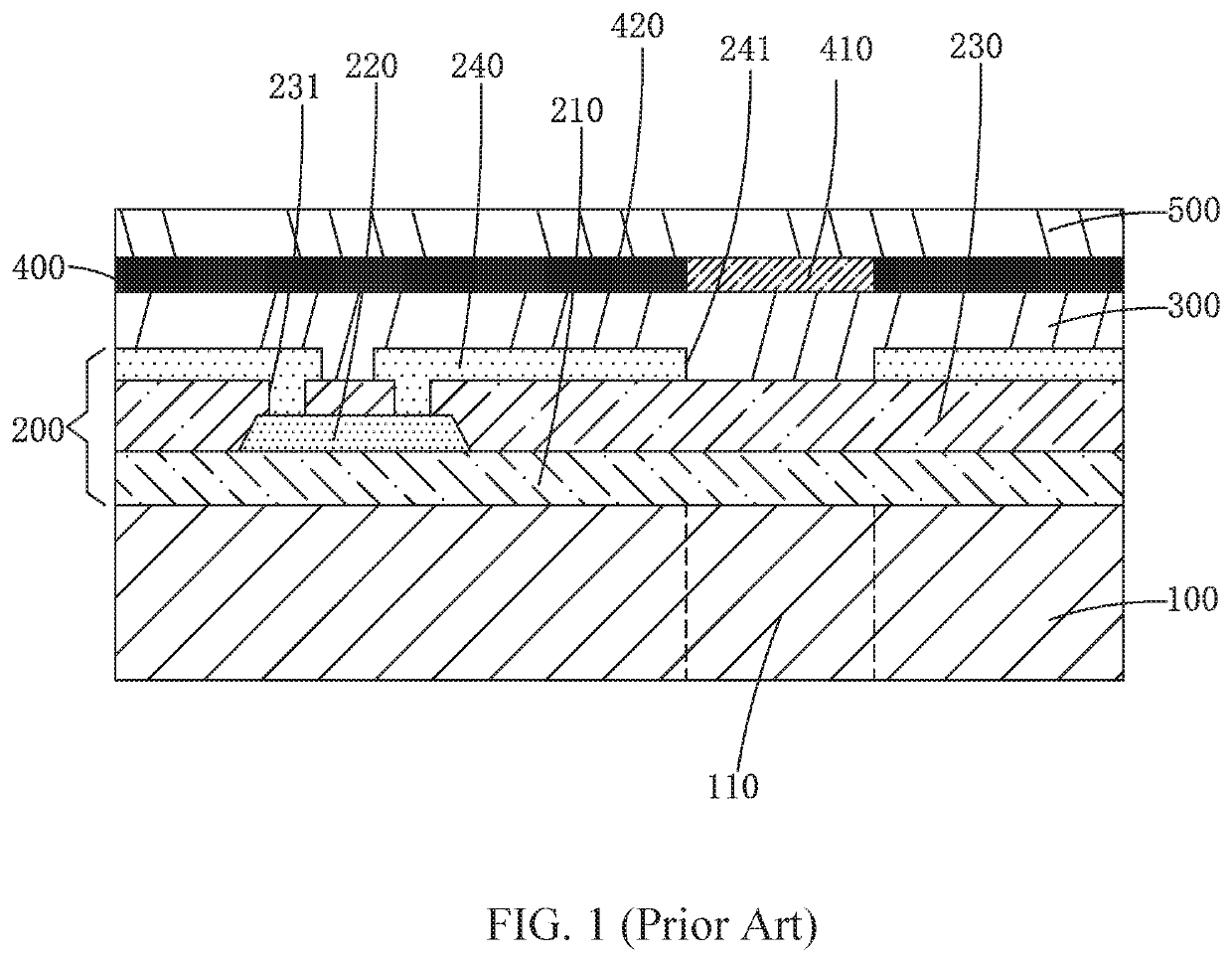
Such an anti-reflection method may lose light and reduce a lifespan of the OLED display device, resulting in a polarizer having a thick thickness and made of a brittle material, not beneficial to development of dynamic bending display panels.
Therefore, number of photomasks required for the manufacturing process is large, resulting in high product cost.

Method used


Image

  • OLED display device and manufacturing method thereof
  • OLED display device and manufacturing method thereof
  • OLED display device and manufacturing method thereof

Examples


Embodiment Construction

[0032]In order to further clarify the technical solutions and effects of the present invention, the following detailed description will be made in conjunction with the preferred embodiments of the invention and the accompanying drawings

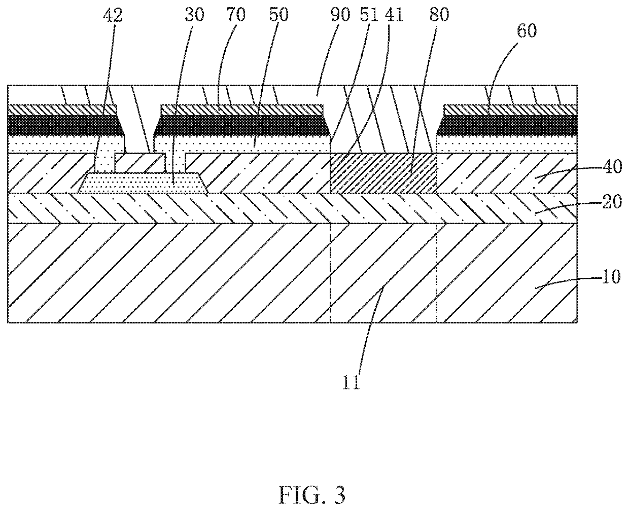
[0033]Please refer to FIG. 2. A first embodiment of the present invention provides an organic light emitting diode (OLED) display device including an OLED display panel 10, a first insulating layer 20 disposed on the OLED display panel 10, a first metal layer 30 disposed on the first insulating layer 20, a second insulating layer 40 disposed on the first metal layer 30 and the first insulating layer 20, a second metal layer 50 disposed on the second insulating layer 40, a black matrix 60 disposed on the second metal layer 50, a hard mask 70 disposed on the black matrix 60, and a plurality of color resists 80 disposed on the OLED display panel 10. One side of the first insulating layer 20 is provided to be a light emitting side for the OLED display pan...


PUM


Abstract

An organic light emitting diode (OLED) display device includes an OLED display panel, a first insulating layer disposed on the OLED display panel, a first metal layer disposed on the first insulating layer, a second insulating layer disposed on the first metal layer and the first insulating layer, a second metal layer disposed on the second insulating layer, a black matrix disposed on the second metal layer, a hard mask disposed on the black matrix, and color resists disposed on the OLED display panel. The OLED display panel includes sub-pixels. Openings extend through the second metal layer, the black matrix, and the hard mask and are positioned corresponding to the sub-pixels. Each color resist is disposed in the openings. The present invention can effectively eliminate reflective light under strong light, and provide a manufacturing process implemented with a small number of masks at a lower product cost.

Description

BACKGROUND OF INVENTION1. Field of Invention[0001]The present invention relates to a technical field of displays, and particularly to, an organic light emitting diode (OLED) display device and a manufacturing method thereof.2. Related Art[0002]Organic light emitting diodes (OLEDs) display devices have been regarded as the most potential development display devices due to advantages of being self-luminous, low driving voltages, high luminous efficiency, quick response times, high definition and contrast, nearly 180° wide viewing angles, and wide temperature range in use, and fulfilling flexible displays and large area and full-color displays.[0003]OLEDs can be classified into two types: passive matrix OLEDs (PMOLEDs) and active matrix OLED (AMOLEDs). That is, a direct addressing type and a thin film transistor (TFT) matrix addressing type, wherein an AMOLED have pixels arranged in arrays, belonging to an active display type and having high luminous efficiency, generally used as high-...

Claims


Application Information

Patent Timeline
IPC IPC(8): H01L51/52H01L27/32H01L51/00H01L51/56G06F3/045
CPCH01L51/56H01L51/5284G06F3/045H01L51/0018H01L2251/56H01L2251/566G06F2203/04103H01L27/323H01L27/322H10K59/35H10K59/38H10K71/233H10K59/8792H10K71/00H10K50/865H10K59/40H10K71/851
Inventor WANG, LEIXIANYU, WENXUGONG, WENLIANGHUANG, XIAOWENCHEN, ZESHENG
Owner WUHAN CHINA STAR OPTOELECTRONICS SEMICON DISPLAY TECH CO LTD
Learn More