Electrostatic discharge protection device

a protection device and electrostatic discharge technology, applied in the direction of semiconductor devices, electrical apparatus, transistors, etc., can solve the problems of internal circuit damage, inability to achieve protection effect, damage to the circuit in the integrated circuit, etc., to prevent latch-up problems, effective prevent internal circuit damage, and lower the trigger voltage

Active Publication Date: 2020-09-24
MACRONIX INT CO LTD
View PDF0 Cites 1 Cited by
  • Summary
  • Abstract
  • Description
  • Claims
  • Application Information

AI Technical Summary

Benefits of technology

[0025]Based on the above, in the ESD protection device according to the invention, the first PNP BJT can lower the trigger voltage of the ESD protection device, thereby effectively preventing internal circuit damage. Furthermore, the first PNP BJT can raise the holding voltage of the ESD protection device to prevent the latch-up issues. Moreover, after the NPN BJT and the second PNP BJT are triggered, the uniformity of current distribution when the ESD protection device is turned on can be improved and the anti-static performance can be improved.

Problems solved by technology

Electrostatic discharge would cause damage to the circuits in an integrated circuit.
However, the ESD protection device currently applied to medium and high voltage semiconductor devices has a high trigger voltage, so that the protection effect cannot be achieved, and the internal circuit is damaged.
Furthermore, the abovementioned has a low holding voltage, and thus is liable to cause latch-up issues, resulting in inoperability of the semiconductor element.

Method used


Image

  • Electrostatic discharge protection device
  • Electrostatic discharge protection device
  • Electrostatic discharge protection device

Examples


Embodiment Construction

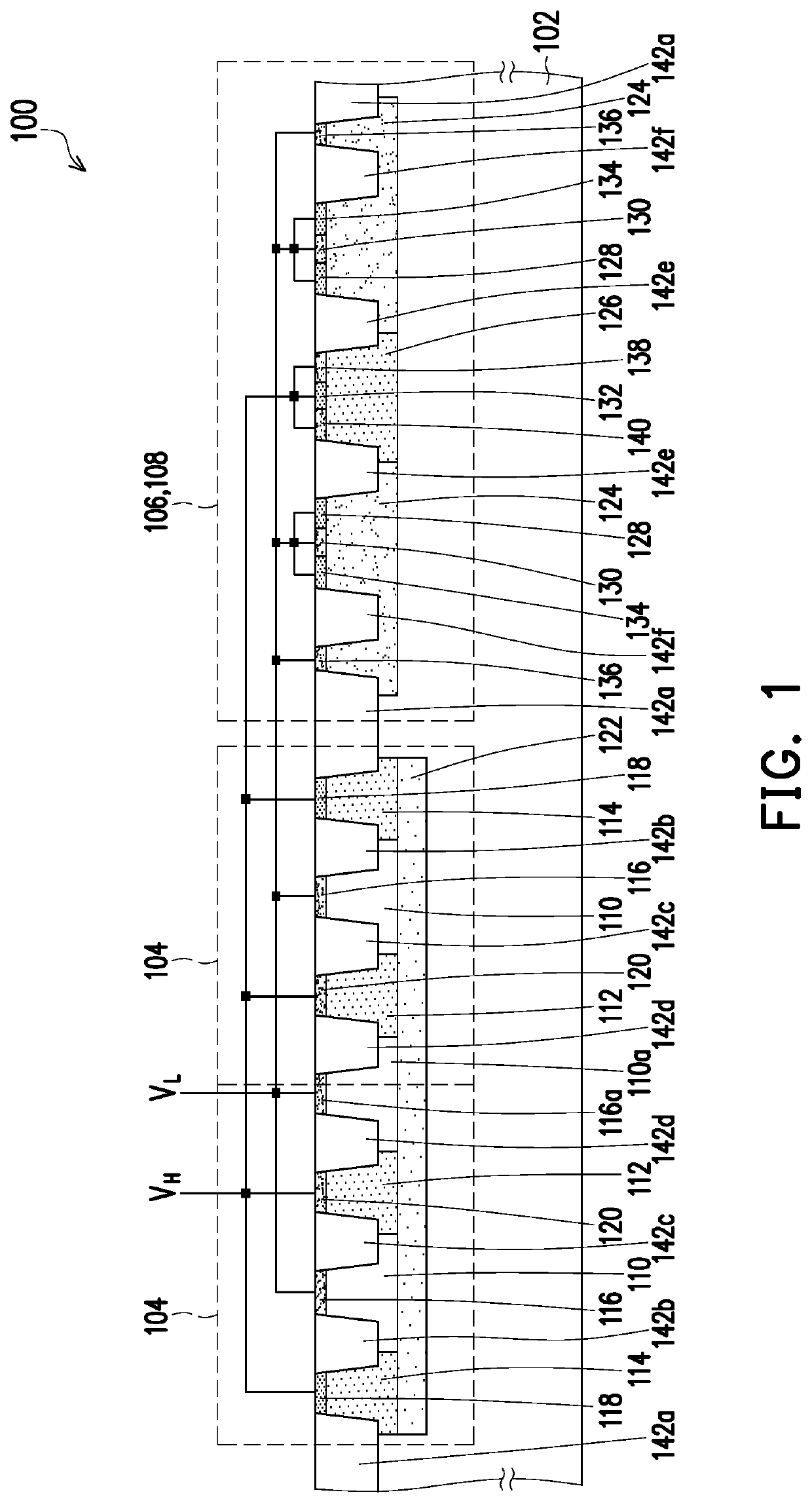
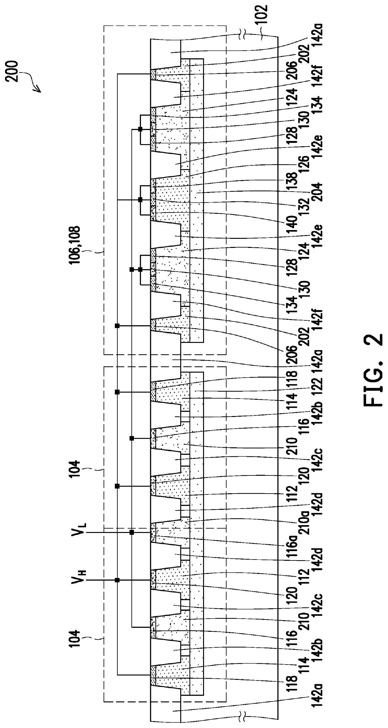
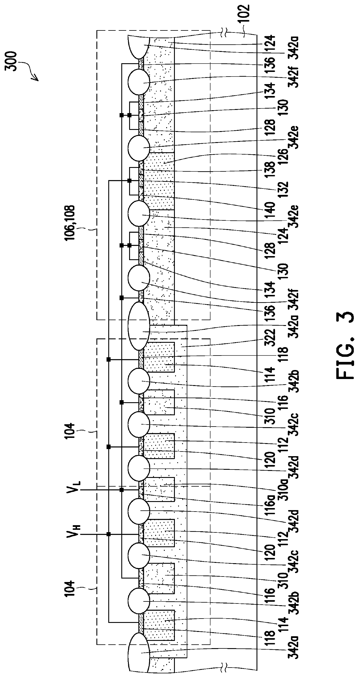
[0031]FIG. 1 is a cross-sectional view illustrating an ESD protection device according to an embodiment of the invention.

[0032]Referring to FIG. 1, an ESD protection device 100 includes a substrate 102, at least one first PNP BJT 104, at least one NPN BJT 106, and at least one second PNP BJT 108. The ESD protection device 100 may be applied to various integrated circuits. For example, the ESD protection device 100 may be applied to medium and high voltage semiconductor devices, but the invention is not limited thereto. The substrate 102 is, for example, a P-type substrate. The substrate 102 is, for example, a single crystal silicon substrate, an epitaxial silicon substrate, or a semiconductor-on-insulator (SOI) substrate.

[0033]The first PNP BJT 104 includes a P-type region 110, an N-type well region 112, an N-type well region 114, a P-type doped region 116, an N-type doped region 118, and a P-type doped region 120, and an N-type region 122. The P-type region 110 is located in the su...


PUM

PropertyMeasurementUnit
voltageaaaaaaaaaa
timeaaaaaaaaaa
holding voltageaaaaaaaaaa

Abstract

An electrostatic discharge protection device including the following components is provided. A first PNP BJT includes a P-type region, first and second N-type well regions, first P-type, first N-type, and second P-type doped regions, and an N-type region. An NPN BJT includes first P-type and third N-type well regions, a second N-type doped region, a third P-type doped region, and a third N-type doped region. A second PNP BJT includes the first P-type and third N-type well regions, the third P-type doped region, the third N-type doped region, and a fourth P-type doped region. The second P-type doped region, the first N-type doped region, the third N-type doped region, and the fourth P-type doped region are coupled to a high voltage side terminal. The first P-type doped region, the second N-type doped region, and the third P-type doped region are coupled to a low voltage side terminal.

Description

BACKGROUND OF THE INVENTIONField of the Invention[0001]This invention relates to a semiconductor device, and particularly relates to an electrostatic discharge protection device.Description of Related Art[0002]Electrostatic discharge (ESD) refers to a phenomenon that charges accumulated in a non-conductor or a non-grounded conductor, and then rapidly moved and discharged through a discharge path in a short time. Electrostatic discharge would cause damage to the circuits in an integrated circuit. Therefore, an ESD protection device is usually placed in the integrated circuit to prevent damage caused by electrostatic discharge.[0003]However, the ESD protection device currently applied to medium and high voltage semiconductor devices has a high trigger voltage, so that the protection effect cannot be achieved, and the internal circuit is damaged. Furthermore, the abovementioned has a low holding voltage, and thus is liable to cause latch-up issues, resulting in inoperability of the sem...

Claims


Application Information

Patent Timeline
Patent Type & Authority Applications(United States)
IPC IPC(8): H01L27/02H02H9/04
CPCH02H9/046H01L27/0248H01L27/0262
Inventor CHAN, WING-CHORCHEN, CHE-HONG
Owner MACRONIX INT CO LTD
Why Eureka
Try Eureka