Light emitting diode package

a technology of light-emitting diodes and packages, applied in the field of packages, can solve the problems of reducing the performance of light-emitting diodes, tarnishing and reducing performance, silver-based materials, and not only expensive, so as to reduce the exposure of electrical conductors, diminishing performance, and reduce the risk of tarnish.

Inactive Publication Date: 2020-10-01
KORRUS INC
View PDF0 Cites 4 Cited by
  • Summary
  • Abstract
  • Description
  • Claims
  • Application Information

AI Technical Summary

Benefits of technology

[0010]The present invention involves, in one embodiment, using a dimensionally-stable substrate with a flip-chip LED and a reflective coating to minimize exposure of electrical conductors in the package. Specifically, Applicants have discovered that by using a substrate material, such as a ceramic, that is dimensionally stable through a wide range of temperatures for the bulk of the submount, the thermal expansion differences in the package can be minimized, thereby facilitating a more robust bond between the LED chip and the pads on the submount.
[0011]Additionally, Applicants have discovered that, while a flip-chip configuration presents certain challenges in connection with the integrity of the electrical connections between the submount and the LED chip as discussed above, it also provides some unexpected benefits. For example, because the chip is upside down, it essentially covers the electrical interface with the submount, which is often a point of diminished reflectivity in the LED package. A flip-chip architecture also provides excellent heatsinking for the LED.
[0012]In one configuration, the present invention provides for a package in which relatively small pads are provided on the surface of the submount to effect an electrical coupling between the LED chip and the electrically-conductive traces in the submount. The small pads are concealed by the flipped chip. Because the electrical connection between the traces and the LED chip is through the pads, the rest of the traces can be covered / concealed by a material which is reflective, but not necessarily conductive. In other words, in one embodiment, there is no need to coat the traces with a material, such as silver, which is used to enhance the traces' reflectivity without diminishing conductivity. (As mentioned above, materials such as silver, which are conductive and reflective, are not only expensive, but also tend to tarnish and diminish performance, especially if certain silicon encapsulants are used because of a violet LED.) Accordingly, Applicants have developed a configuration in which the LED packaging has essentially no exposed traces which would otherwise diminish the package's reflectivity.
[0013]In another embodiment, traces are coated with a material, such as silver, which provides reflectivity and conductivity, but the material is coated with barrier to protect the material from corrosion while not diminishing its reflectiveness. Again, a package configuration is provided in which the LED packaging has essentially no exposed traces, which would otherwise diminish the package's reflectivity.
[0016]In still another embodiment, an LED package is disclosed having a flip chip connected to a conductor, which is covered by a conductive and reflective material, which is further coated with a barrier layer to prevent corrosion. In one embodiment, the LED package comprises: (a) a substrate; (b) at least one electrical conductor disposed on the substrate; (c) a reflective material disposed over a major portion of the at least one electrical conductor; (d) a protective layer disposed over a portion of the reflective material; and (e) a violet LED chip having at least one contact, the at least one contact being electrically connected to the at least one electrical conductor through the reflective layer.

Problems solved by technology

For example, because the chip is upside down, it essentially covers the electrical interface with the submount, which is often a point of diminished reflectivity in the LED package.
(As mentioned above, materials such as silver, which are conductive and reflective, are not only expensive, but also tend to tarnish and diminish performance, especially if certain silicon encapsulants are used because of a violet LED.)

Method used


Image

  • Light emitting diode package
  • Light emitting diode package
  • Light emitting diode package

Examples


Embodiment Construction

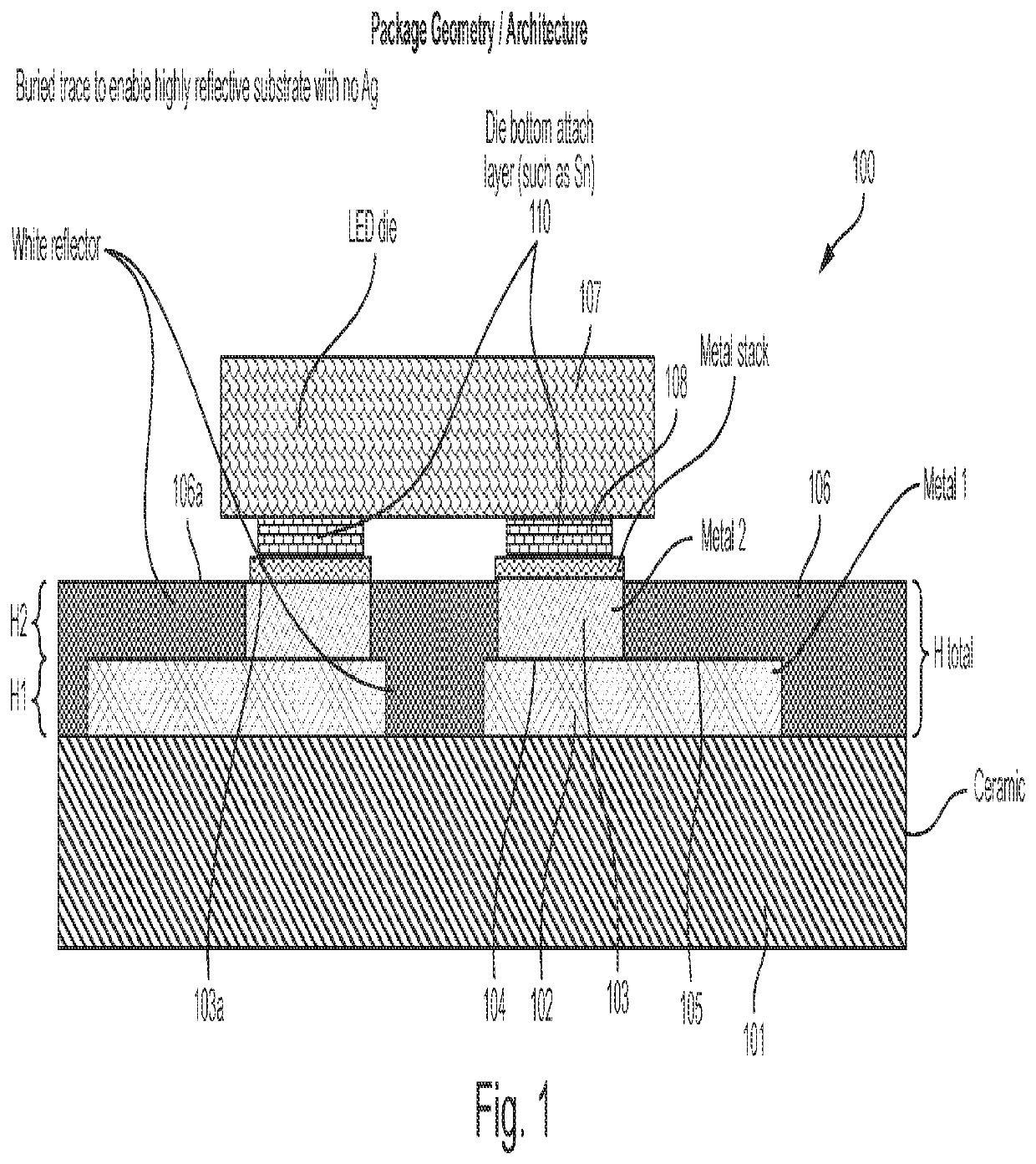
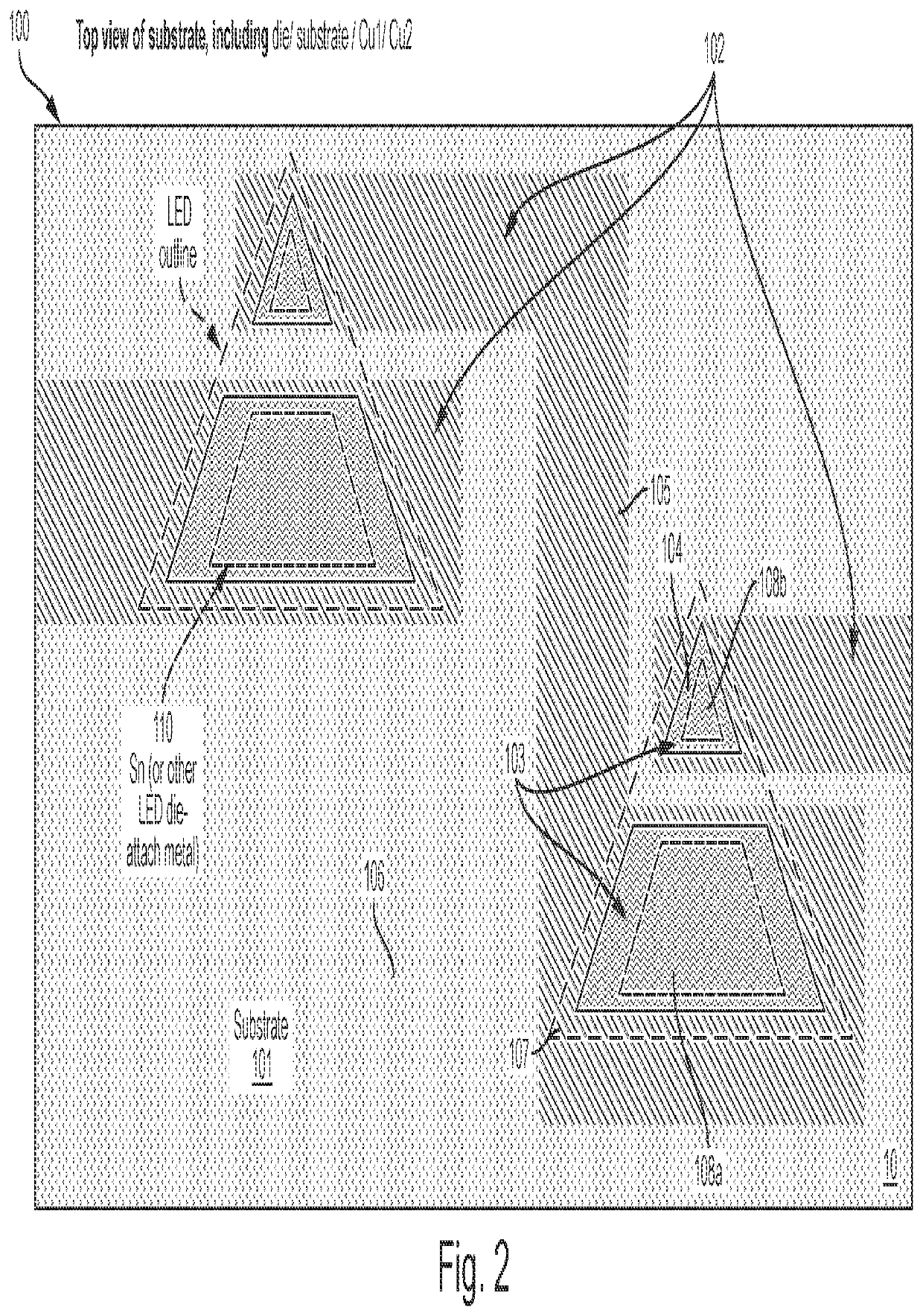
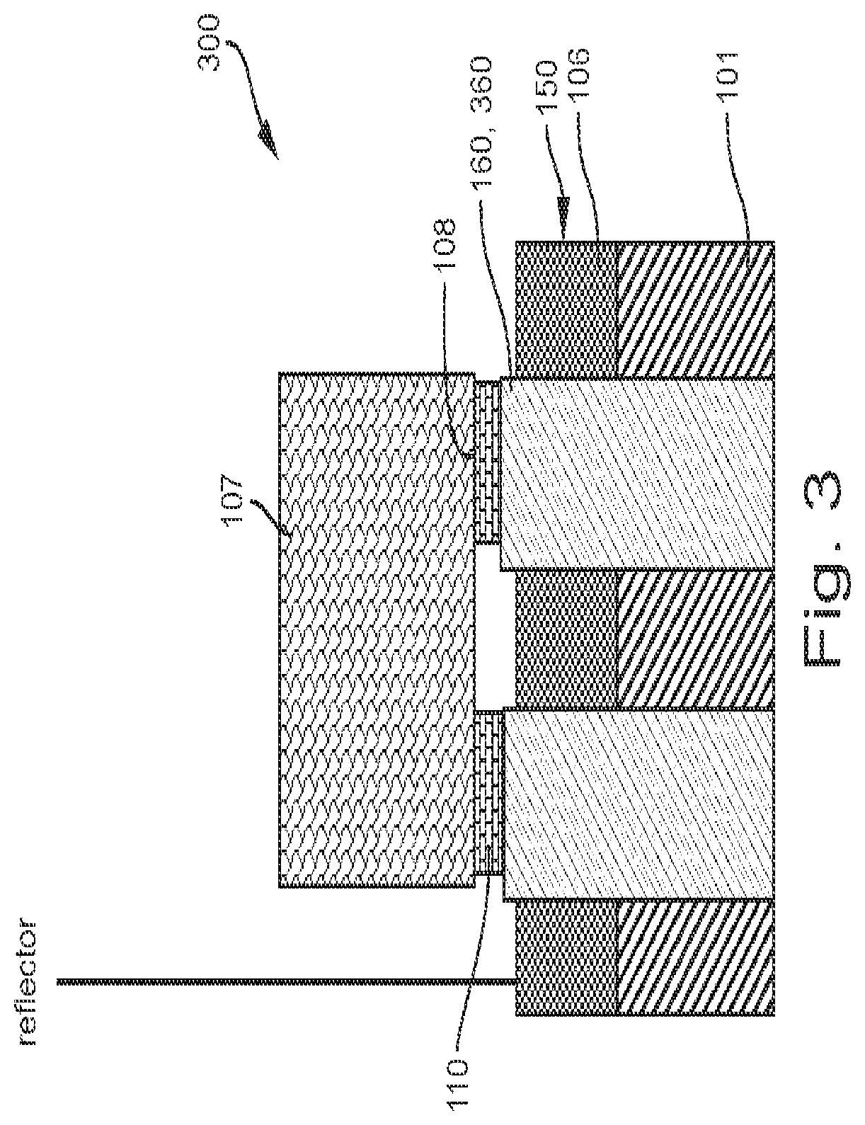
[0045]Referring to FIG. 1, one embodiment of an LED package 100 of the present invention is shown. The package 100 comprises a submount 150 comprising a substrate 101, at least one electrical interface 160, and a non-conductive reflective material 106 disposed over substantially all of the submount except for the at least one electrical interface. The package also comprises an LED chip 107 having sides 120 and at least one contact 108. The LED chip is flip-chip mounted to the submount such that the at least one contact is electrically connected to the at least one electrical interface. When mounted, the LED chip covers a substantial portion of the at least one electrical interface, and substantially all of the chip extends above the reflective material. The elements / features of this embodiment are described in greater detail below.

[0046]An important feature of this embodiment is that the area of the electrical interface 160 on the surface of the submount 150 is relatively small, the...


PUM

PropertyMeasurementUnit
wavelengthsaaaaaaaaaa
reflectivityaaaaaaaaaa
thicknessaaaaaaaaaa

Abstract

In one embodiment, the LED package comprises: (a) a submount comprising a substrate, at least one electrical interface, and a non-conductive reflective material disposed over substantially all of submount except for the at least one electrical interface; and (b) an LED chip having sides and at least one contact, the LED chip being flip-chip mounted to the submount such that the at least one contact is electrically connected to the at least one electrical interface, the LED chip covering a substantial portion of the at least one electrical interface, substantially all of the chip extending above the reflective material.

Description

RELATED APPLICATION[0001]This application is based on U.S. Provisional Application No. 62 / 352,864, filed Jun. 21, 2016, hereby incorporated by reference in its entirety.FIELD OF INVENTION[0002]The present invention relates, generally, to a package, and, more specifically, to a light emitting diode (LED) package suitable for shorter-wavelength LEDs.BACKGROUND[0003]Conventional mid-power packages (MPP) use leadframe architecture with a wire-bonded die and exposed silver for high optical reflectivity. Typically, blue pump LEDs are employed and are encapsulated in a phenyl-based silicone. Such silicones have a rather high index (˜1.5) and tend to protect the silver against corrosion / tarnishing.[0004]Although such MPPs may be sufficient for blue, wire-bonded LEDs, Applicants have identified a number of shortcomings of such packages for shorter wavelength LEDs and for flip-chip packages. (As used herein short-wavelength light comprises light at a wavelength significantly shorter than stan...

Claims


Application Information

Patent Timeline
Patent Type & Authority Applications(United States)
IPC IPC(8): H01L33/54H01L33/62H01L33/46H01L33/60H01L33/48
CPCH01L33/60H01L33/54H01L33/62H01L33/46H01L33/486H01L25/0753H01L33/20H01L2224/16225H01L2933/0058H01L2933/0066
Inventor HUANG, KEVINDAVID, AURELIEN J.F.EBERLE, STEFANMODI, ROHITWEST, SCOTTCICH, MICHAEL J.ALDAZ, RAFAEL I.CRAVEN, MICHAEL D.
Owner KORRUS INC
Why Eureka
Try Eureka