Image sensor and electronic device including image sensor

Active Publication Date: 2020-12-24
SAMSUNG ELECTRONICS CO LTD
View PDF0 Cites 3 Cited by
  • Summary
  • Abstract
  • Description
  • Claims
  • Application Information

AI Technical Summary

Benefits of technology

[0005]One or more example embodiments provide an image sensor that is able to improve an autofocus performance of a peripheral

Problems solved by technology

However, angles of incident lights may not be separate

Method used


Image

  • Image sensor and electronic device including image sensor
  • Image sensor and electronic device including image sensor
  • Image sensor and electronic device including image sensor

Examples


Example

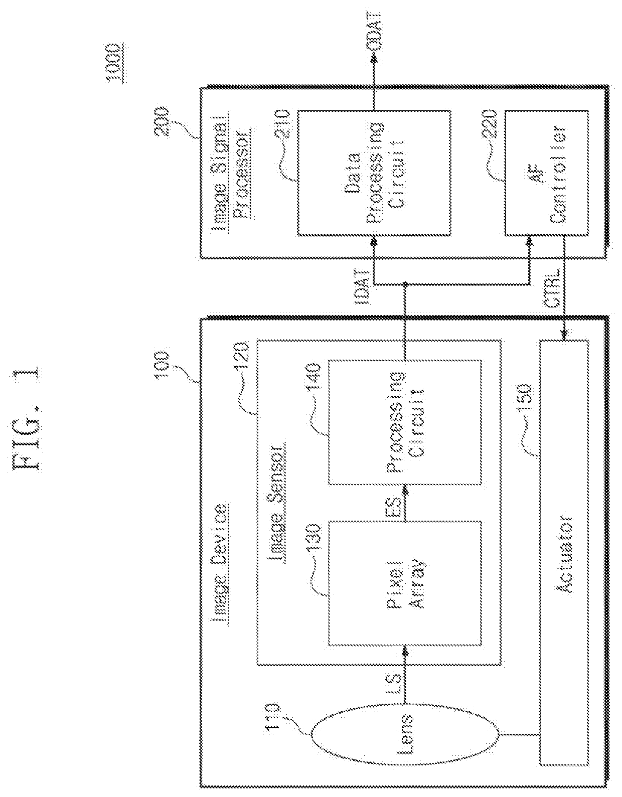
[0022]FIG. 1 is a block diagram illustrating an image system according to an example embodiment. Referring to FIG. 1, an image system 1000 includes an image device 100 and an image signal processor (ISP) 200. For example, the image system 1000 may be one of various electronic devices, which are able to obtain image information about an object from the outside, such as a smartphone, a tablet PC, and a digital camera.

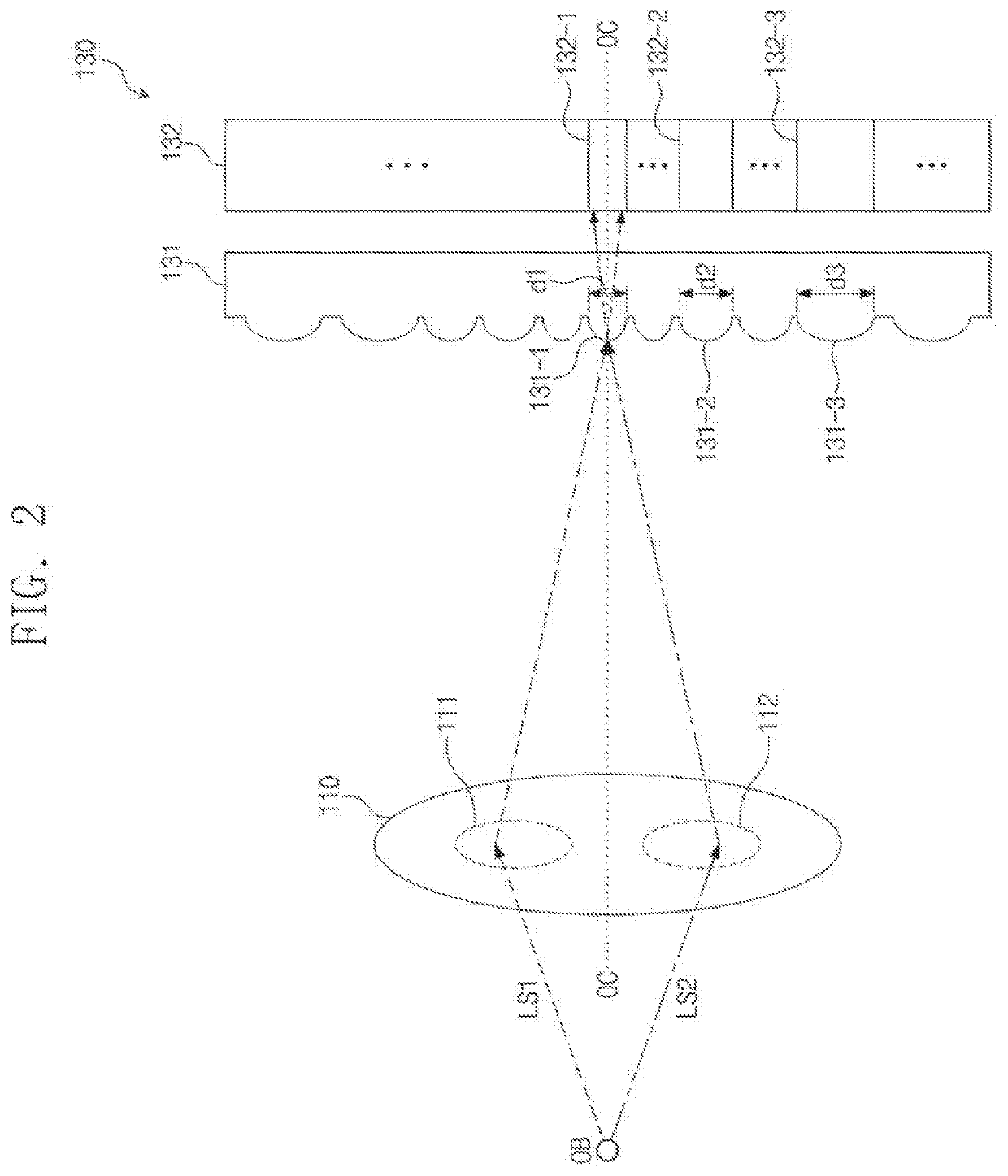
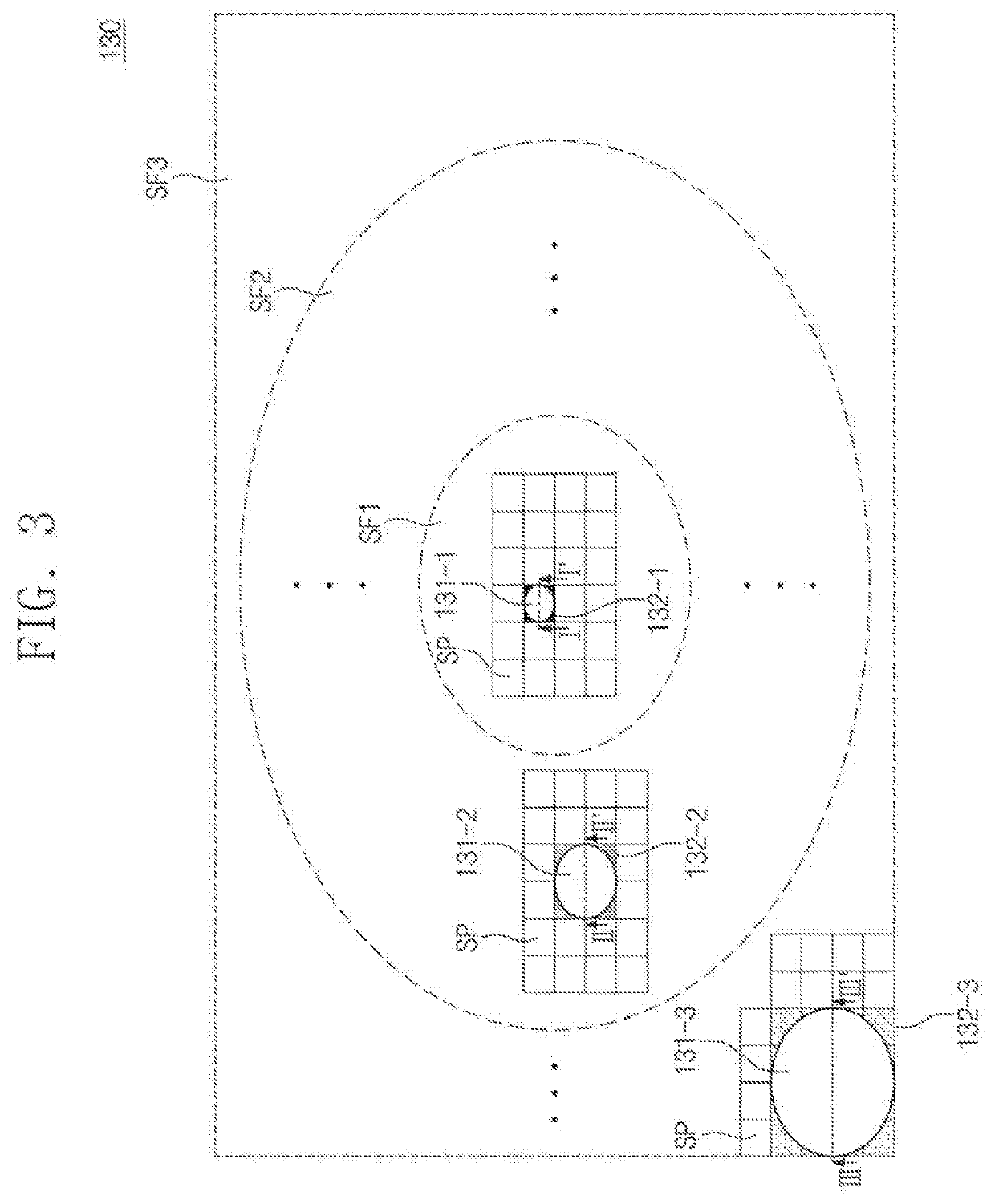
[0023]The image device 100 may include a lens 110, an image sensor 120, and an actuator 150. The image sensor 120 may include a pixel array 130 and a processing circuit 140.

[0024]The lens 110 may receive a light LS that is incident after being reflected from an external object. The lens 110 may concentrate the received light signal LS on the pixel array 130. The lens 110 may move based on an operation of the actuator 150. When a location of the lens 110 varies depending on the movement of the lens 110, a focal distance of the lens 110 may change to get an object in focus....


PUM


Abstract

Provided is an image sensor including a pixel array including a plurality of pixels, and a micro lens array including a first micro lens of a first size provided in a first area of the pixel array and a second micro lens of a second size provided in a second area of the pixel array, the second size being different from the first size.

Description

CROSS-REFERENCE TO THE RELATED APPLICATION[0001]This application claims priority from Korean Patent Application No. 10-2019-0073066 filed on Jun. 19, 2019, in the Korean Intellectual Property Office, the disclosure of which is incorporated herein by reference in its entirety.BACKGROUND1. Field[0002]Example embodiments of the present disclosure relate to an electronic device, and more particularly, to an image sensor and an electronic device including the image sensor.2. Description of the Related Art[0003]An image sensor included in a smartphone, a tablet personal computer (PC), or a digital camera obtains image information about an external object by converting a light reflected from the external object into an electrical signal. An autofocus (AF) may be performed to improve the quality of image of the external object. For faster autofocus, an image sensor that supports a phase detection autofocus (PDAF) may be used.[0004]The image sensor that supports the PDAF may receive an incid...

Claims


Application Information

Patent Timeline
IPC IPC(8): H04N5/232H04N5/225
CPCH04N5/232122H04N5/2254H01L27/14605H01L27/14627H01L27/14634H01L27/14621H04N23/67H04N23/672H04N25/70H04N23/55H04N25/704
Inventor NOH, YOHWANKIM, DAEKWANKIM, CHAESUNGWANG, TAE-SHICK
Owner SAMSUNG ELECTRONICS CO LTD
Why Eureka
Try Eureka