Thin film type solar cell and method for manufacturing the same

a solar cell and film technology, applied in the direction of basic electric elements, electrical equipment, semiconductor devices, etc., can solve the problems of increased manufacturing costs, disadvantageous increase of power loss, and limitation of minimizing thickness during processes, and achieve superior photoelectric transformation efficiency and advantageously obtain more electric energy

Inactive Publication Date: 2021-01-07
JUSUNG ENG
View PDF0 Cites 0 Cited by
  • Summary
  • Abstract
  • Description
  • Claims
  • Application Information

AI Technical Summary

Problems solved by technology

The substrate type solar cell exhibits slightly superior efficiency, but has a limitation in minimizing a thickness during processes, and a disadvantage of increased manufacturing costs due to use of an expensive semiconductor substrate as a thin film type solar cell.
As the area of the substrate increases, power loss is disadvantageously increased due to the resistance of transparent conductive material.

Method used


Image

  • Thin film type solar cell and method for manufacturing the same
  • Thin film type solar cell and method for manufacturing the same
  • Thin film type solar cell and method for manufacturing the same

Examples


first embodiment

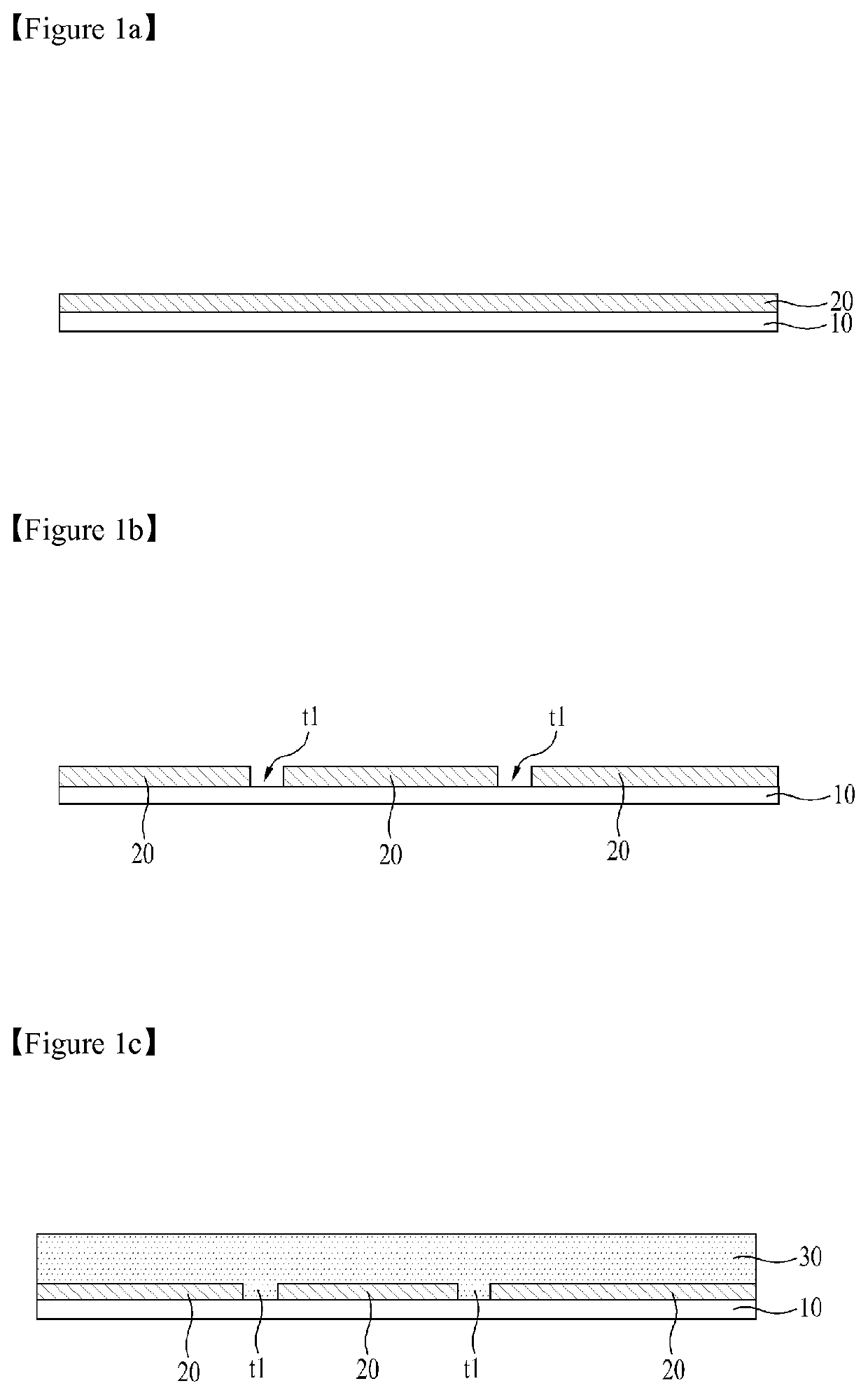
[0121]As shown in FIG. 5A, in the present invention, a connection member 133 is formed in the unit cell such that the first semiconductor layer 131 and the second semiconductor layer 132 arranged at both sides of the second trench P2 are not entirely divided through the second trench P2.

[0122]That is, when the second trench P2 is formed by laser scribing, a part of the region provided between the first semiconductor layer 131 and the second semiconductor layer 132 is left to prevent complete separation of the first semiconductor layer 131 and the second semiconductor layer 132.

[0123]Although the region between the first semiconductor layer 131 and the second semiconductor layer 132 should be removed in order to form the second trench P2, laser scribing is preformed while excluding a part of the semiconductor layer 130 to form the connection member 133.

[0124]The connection member 133 is arranged at one side of the second trench P2 and extension of the second trench P2 is thus blocked...

second embodiment

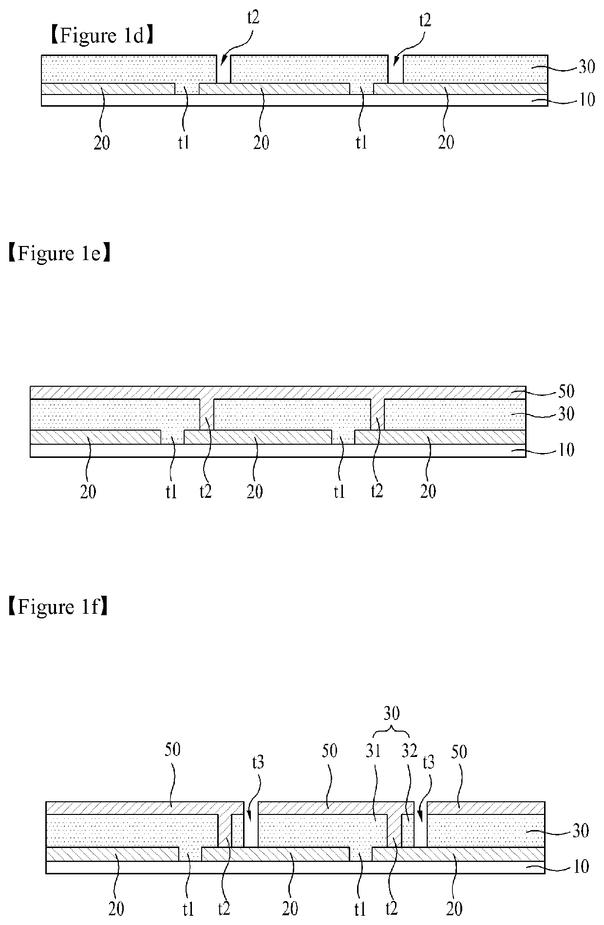
[0146]In a second embodiment, the first semiconductor layer 231 is connected to the second semiconductor layer 232 through two connection members 233.

[0147]A plurality of connection members 233 are spaced from one another in one unit cell.

[0148]As shown in FIG. 6, the connection members 233 may be formed at both sides of the second trench P2, or may be spaced from one another such that they cross the second trench P2.

[0149]In this case, the total length of connection members 233 arranged at both ends is preferably maintained to 1 / 10 or less of the length of the third trench P3.

[0150]The second trench P2 is surrounded by the first and second semiconductor layers 231 and 232, and the connection member 233 and may have a groove shape in which upper and lower parts thereof open and four surfaces thereof close.

[0151]As shown in FIG. 6(B), the first trench P1 and the third trench P3 extend to the fourth trench P4, while the second trench P2 does not extend to the fourth trench P4.

[0152]Ac...


PUM

PropertyMeasurementUnit
temperatureaaaaaaaaaa
frequencyaaaaaaaaaa
sizeaaaaaaaaaa

Abstract

Disclosed is a thin film type solar cell with superior efficiency and a method for manufacturing the same.
The thin film type solar cell includes a substrate, one or more front electrodes arranged on the substrate such that the front electrodes are spaced from one another through a first trench, a semiconductor layer arranged on the front electrode, wherein a part of the semiconductor layer is removed by a second trench adjacent to the first trench, and one or more rear electrodes arranged on the second trench and the semiconductor layer such that the rear electrodes are spaced from one another through a third trench adjacent to the second trench, wherein the semiconductor layer include one or more connection members which are adjacent to the second trench and are divided by the second trench.
Based on such configuration, the thin film type solar cell and the method for manufacturing the same provide superior photoelectric transformation efficiency by connecting semiconductor layers arranged at both sides of the second trench through the connection member.

Description

TECHNICAL FIELD[0001]The present invention relates to a thin film type solar cell with superior efficiency and a method for manufacturing the same.BACKGROUND ART[0002]A solar cell is a device which converts light energy into electric energy using semiconductor characteristics.[0003]The structure and principle of solar cell will be described in brief A solar cell has a PN junction structure in which a positive (p)-type semiconductor and a negative (n)-type semiconductor are junctioned.[0004]When solar light is incident upon the solar cell having a structure, holes and electrons are generated in the semiconductor by the energy of incident solar light.[0005]At this time, holes (+) and the electrons (−) move towards the p-type semiconductor and the n-type semiconductor, respectively, by an electric field generated at the PN junction, to produce electricity.[0006]Such a solar cell may be classified into a substrate type solar cell and a thin film type solar cell.[0007]The substrate type ...

Claims


Application Information

Patent Timeline
Patent Type & Authority Applications(United States)
IPC IPC(8): H01L31/0465H01L31/0224H01L31/18
CPCH01L31/0465H01L31/1804H01L31/022433Y02E10/547H01L31/022441H01L31/18H01L31/0445H01L31/047
Inventor MIN, JUN KICHOI, SANG SU
Owner JUSUNG ENG
Why Eureka
Try Eureka