New dual-gate trench IGBT with buried floating p-type shield

a technology of floating shield and trench igbt, which is applied in the direction of semiconductor devices, semiconductor/solid-state device details, electrical apparatus, etc., can solve the problems of high energy dissipation, slow down the igbt device, and still face difficulties and limitations of the transistor (igbt) device, so as to improve the igbt device scalability and the effect of reducing the risk

Active Publication Date: 2021-01-21
ALPHA & OMEGA SEMICON INC
View PDF0 Cites 3 Cited by
  • Summary
  • Abstract
  • Description
  • Claims
  • Application Information

AI Technical Summary

Benefits of technology

[0007]It is therefore an aspect of the present invention to provide a new and improved IGBT device configuration and manufacturing method for providing a trench IGBT device with a du

Problems solved by technology

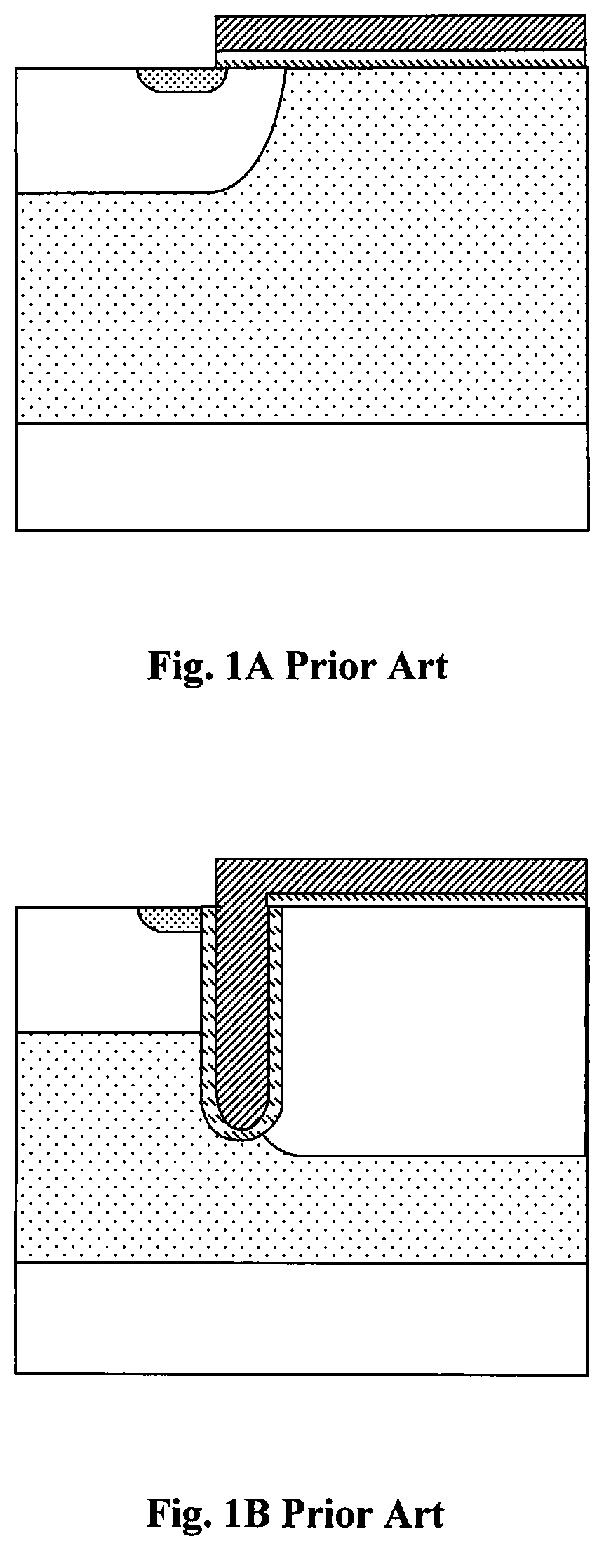
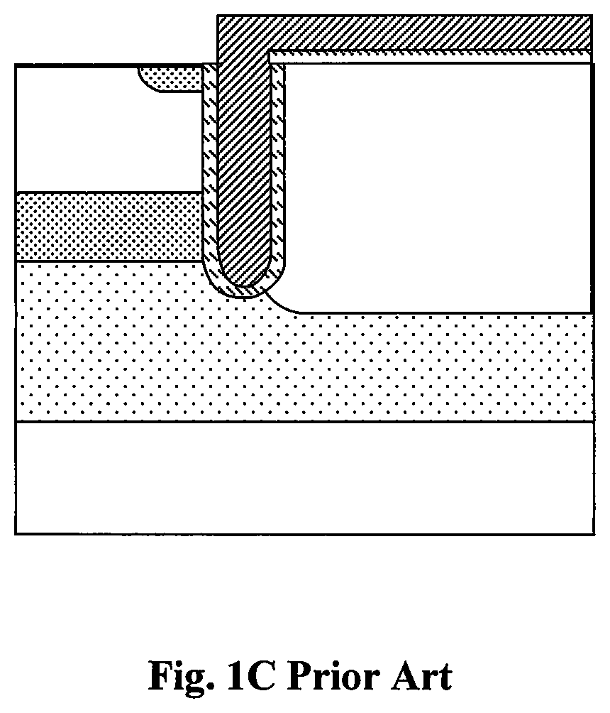
Conventional technologies to configure and manufacture insulated gate bipolar transistor (IGBT) devices are still confronted with difficulties and limitations to further improve the performances due to different tradeoffs.
A high Jsat will result in a lot of energy dissipated in the device during short circuit, which would quickly damage the IGBT device.
A lower Jsat will reduce the amount of energy dissipated, allowing the IGBT device to withstand the short circuit for a longer period of time without permanent damage; however, a lower Jsat also results in higher c

Method used


Image

  • New dual-gate trench IGBT with buried floating p-type shield
  • New dual-gate trench IGBT with buried floating p-type shield
  • New dual-gate trench IGBT with buried floating p-type shield

Examples


Embodiment Construction

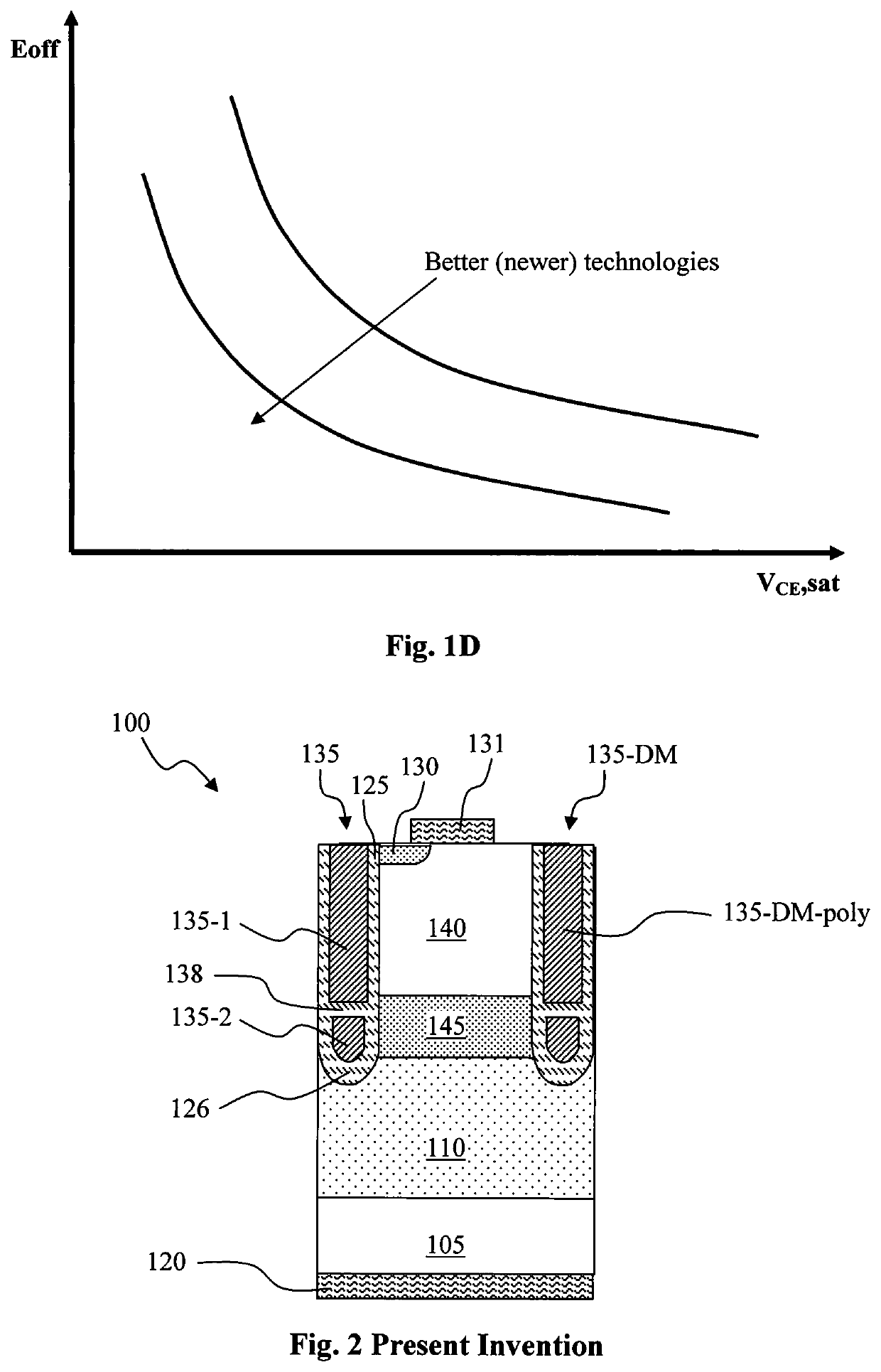
[0038]FIG. 2 is a cross-sectional view of an IGBT device having a trench shield and trench gate configuration with dummy trench of this invention. The IGBT device 100 is formed in semiconductor substrate 105 that has a first conductivity type, e.g., a P type substrate 105. An epitaxial layer 110 of a second conductivity type, e.g. an N− epitaxial (epi) layer 110, is supported on top of the P-type substrate 105. Alternatively, the P type substrate 105 and the epitaxial layer 110 may together be referred to as the semiconductor substrate since they both generally have a mono-crystalline structure; additionally, the P type substrate 105 may be more generally referred to as a bottom or lower semiconductor layer and the epitaxial layer 110 may more generally be referred to as an upper semiconductor layer. The IGBT 100 is a vertical IGBT device with a collector electrode 120 disposed on a bottom surface of the substrate and an emitter electrode 131 disposed on a top surface. The IGBT devi...


PUM


Abstract

A method of manufacturing an insulated gate bipolar transistor (IGBT) device comprising 1) preparing a semiconductor substrate with an epitaxial layer of a first conductivity type supported on the semiconductor substrate of a second conductivity type; 2) applying a gate trench mask to open a first trench and second trench followed by forming a gate insulation layer to pad the trench and filling the trench with a polysilicon layer to form the first trench gate and the second trench gate; 3) implanting dopants of the first conductivity type to form an upper heavily doped region in the epitaxial layer; and 4) forming a planar gate on top of the first trench gate and apply implanting masks to implant body dopants and source dopants to form a body region and a source region near a top surface of the semiconductor substrate.

Description

[0001]This Patent Application is a Divisional Application of a co-pending application Ser. No. 16 / 258,662 and application Ser. No. 16 / 258,662 is a Continuation Application of another application Ser. No. 15 / 600,782 now issued into U.S. Pat. No. 10,199,455 on Feb. 5, 2019. application Ser. No. 15 / 600,782 is a Divisional Application of another application Ser. No. 14 / 712,599 filed on May 14, 2015 now issued into U.S. Pat. No. 9,666,666 on May 30, 2017. Application Ser. No. 14 / 712,599 is a Divisional Application of application Ser. No. 13 / 831,066 filed on Mar. 13, 2013 and issued into U.S. Pat. No. 9,048,282 on Jun. 2, 2015. Application Ser. No. 13 / 831,066 is a Continuation in Part (CIP) Application and claim the Priority Date of a co-pending application Ser. No. 12 / 925,869 filed on Oct. 3, 2010 filed by a Common Inventor of this Application and issued into U.S. Pat. No. 8,933,506 on Jan. 13, 2015.BACKGROUND OF THE INVENTION1. Field of the Invention[0002]The invention relates generally...

Claims


Application Information

Patent Timeline
IPC IPC(8): H01L23/522H01L23/00H01L23/31H01L23/528H01L21/56
CPCH01L23/5226H01L24/09H01L24/17H01L24/33H01L24/73H01L2224/0231H01L23/5283H01L21/561H01L24/97H01L2224/02373H01L2224/02379H01L23/3128H01L21/568H01L23/3114H01L21/6835H01L2221/68327H01L2221/68345H01L2221/68359H01L2221/68372H01L21/6836H01L2224/73267H01L2224/32225H01L2224/04105H01L2224/92244H01L2224/83385H01L2224/83005H01L2924/15311H01L2224/214H01L2223/6677H01L23/66H01L24/19H01L2224/97H01L2224/94H01L24/20H01L24/32H01L24/92H01L24/83H01L2224/83H01L29/1095H01L29/66348H01L29/7393
Inventor HU, JUNBOBDE, MADHURYILMAZ, HAMZA
Owner ALPHA & OMEGA SEMICON INC
Why Eureka
Try Eureka