

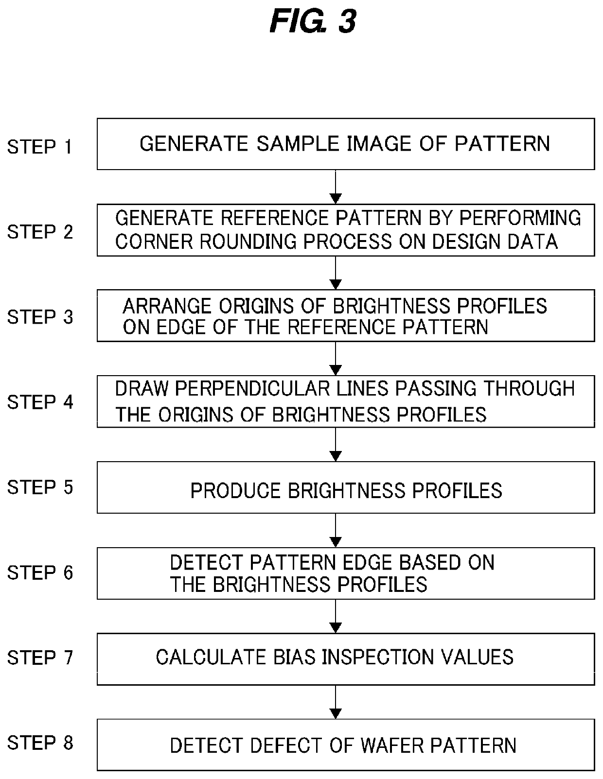
Pattern edge detection method
a detection method and pattern technology, applied in the direction of material analysis using wave/particle radiation, instruments, image enhancement, etc., can solve the problems of not being able to detect patterns formed at a location other than a corner, not being able to detect actual corner rounds as defects, and training data. the effect of improving the accuracy of pattern edge detection using machine learning
- Summary
- Abstract
- Description
- Claims
- Application Information
AI Technical Summary
Benefits of technology
Problems solved by technology
Method used
Image

Examples
Embodiment Construction
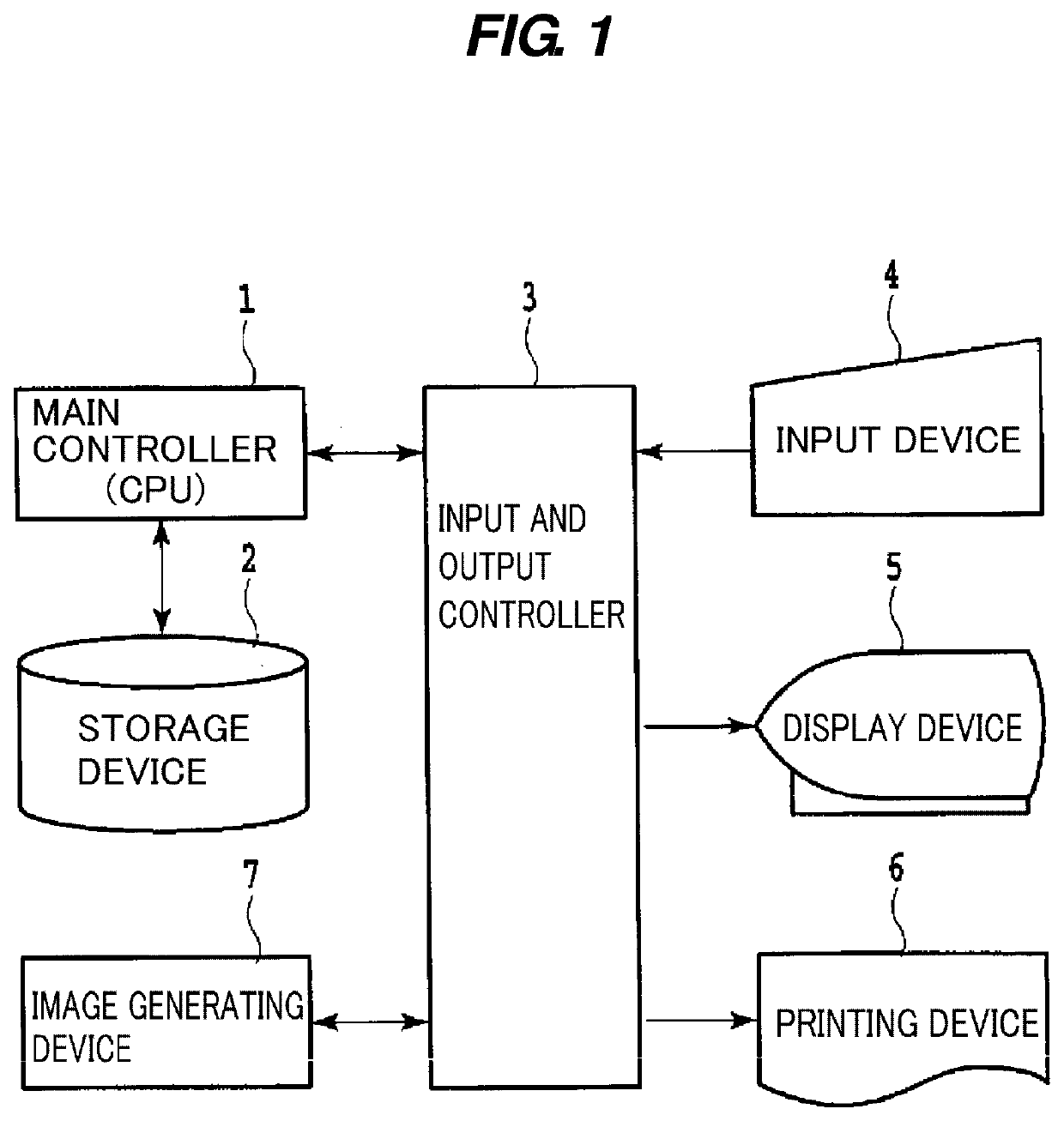
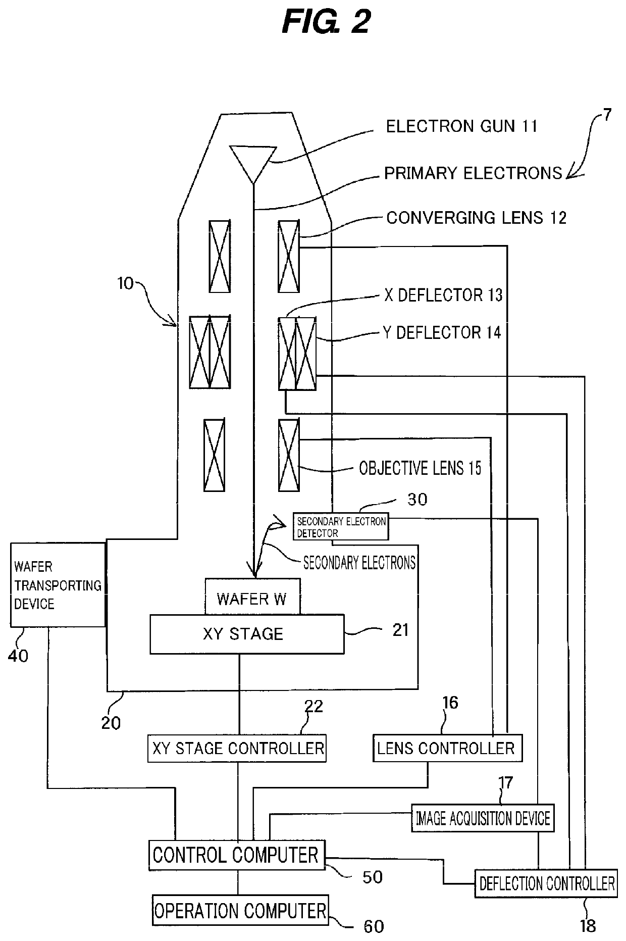
[0064]Embodiments of the present invention will now be described below with reference to the drawings. FIG. 1 is a schematic diagram showing an embodiment of a pattern inspection apparatus. The pattern inspection apparatus according to this embodiment includes a main controller 1, a storage device 2, an input and output controller 3, an input device 4, a display device 5, a printing device 6, and an image generating device 7.
[0065]The main controller 1 includes CPU (Central Processing Unit), and controls the entire apparatus as a whole. The storage device 2 is coupled to the main controller 1. The storage device 2 may be in the form of a hard disk, a solid state drive, a flexible disk, or an optical disk. The input device 4 (e.g., a keyboard and a mouse), the display device 5 (e.g., a display for displaying input data and calculation results), and the printing device 6 (e.g., printer) are coupled to the main controller 1 via the input and output controller 3.
[0066]The main controlle...
PUM
| Property | Measurement | Unit |
|---|---|---|
| semiconductor inspection | aaaaa | aaaaa |
| optical pattern inspection | aaaaa | aaaaa |
| brightness | aaaaa | aaaaa |
Abstract
Description
Claims
Application Information