

Wide-gap semiconductor device
a semiconductor device and wide-gap technology, applied in semiconductor devices, diodes, electrical devices, etc., can solve the problems of abnormal increase of the above-mentioned well region below the gate pad, complicated manufacturing methods, and high manufacturing costs, and achieve the effect of preventing current concentration and abnormal increase of potential
- Summary
- Abstract
- Description
- Claims
- Application Information
AI Technical Summary
Benefits of technology
Problems solved by technology
Method used
Image

Examples
first embodiment
[0039]>
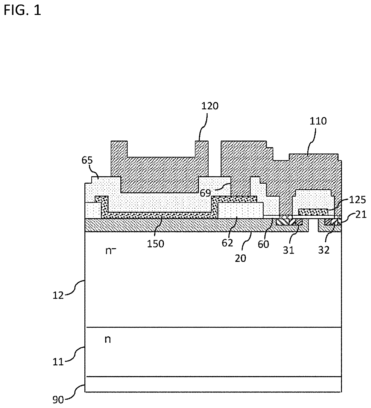
[0040]In the present embodiment, description will be given using a vertical MOSFET as one example. Though it is assumed that a first conductivity type is an n type and a second conductivity type is a p type in the description of the present embodiment, the present invention is not limited to that aspect. It may be set such that a first conductivity type is a p type and a second conductivity type is an n type. Further, though the description will be given using silicon carbide as a wide gap semiconductor in the present embodiment, the present invention is not limited to that aspect. Gallium nitride or the like may be used as a wide gap semiconductor. In the present embodiment, a vertical direction in FIG. 1 (a direction along a width of a wide gap semiconductor device) will be referred to as a vertical direction and a direction perpendicular to the vertical direction will be referred to as an in-plan direction.
[0041]As illustrated in FIG. 1, a silicon-carbide semiconductor dev...
second embodiment
[0070]Next, a second embodiment of the present invention will be described.
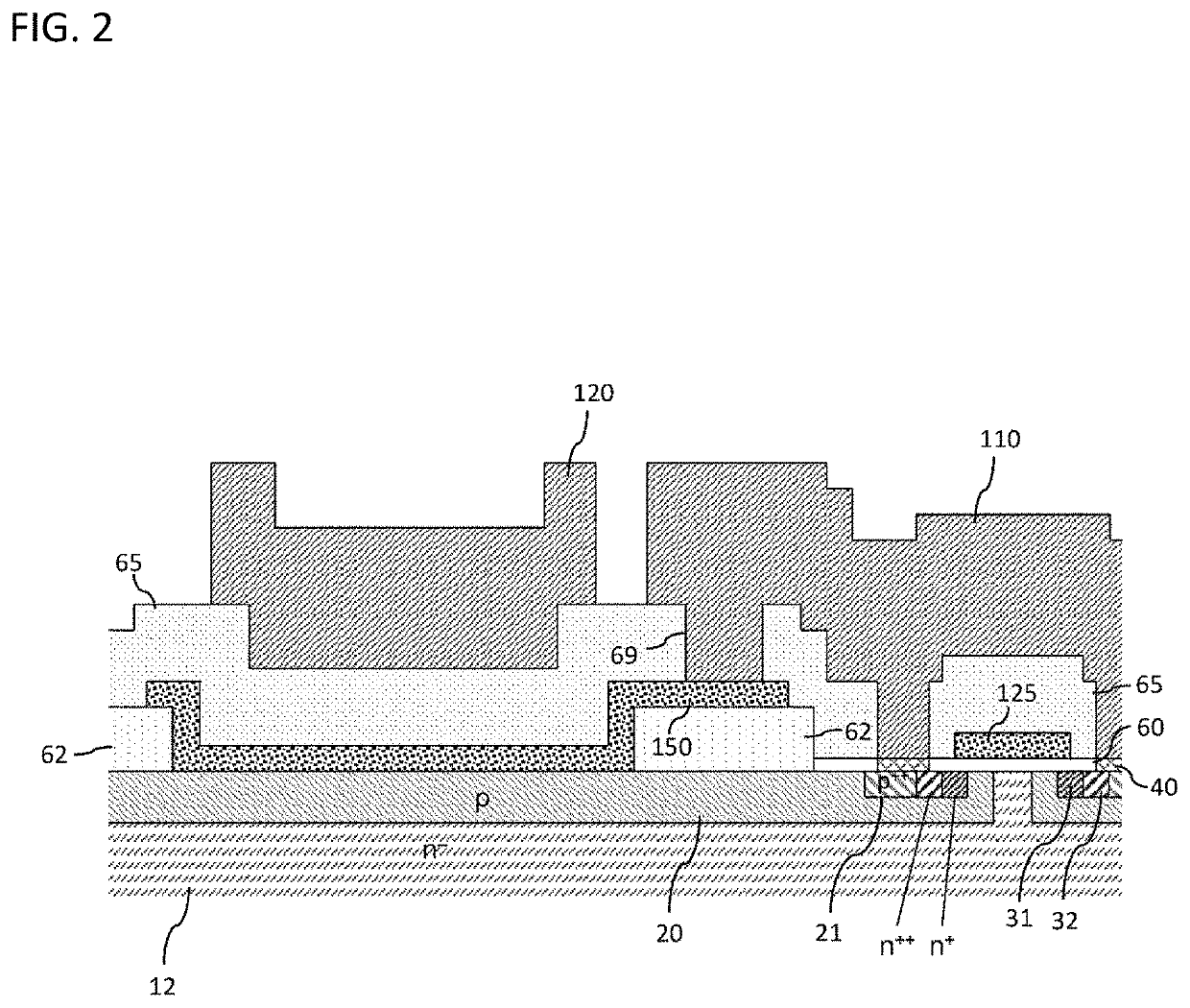
[0071]In the present embodiment, as illustrated in FIG. 4, a polysilicon layer 150 has an undoped polysilicon layer 151 provided on a well region 20 so as to be in contact with the well region 20, and a doped polysilicon layer 152 provided on the undoped polysilicon layer 151. Various configurations employed in the above-described embodiment can be employed also in the third embodiment. The members described in the above embodiment will be described with the same reference signs.
[0072]In a case where doped polysilicon is used as the polysilicon layer 150, particularly in a case where n-type doped polysilicon is used, a Schottky barrier φB is reduced excessively in some cases. In this regard, in the present embodiment, providing the undoped polysilicon layer 151 as a layer in contact with the well region 20 can prevent excessive reduction of a Schottky barrier φB.
[0073]In the present embodiment, it can be cons...
third embodiment
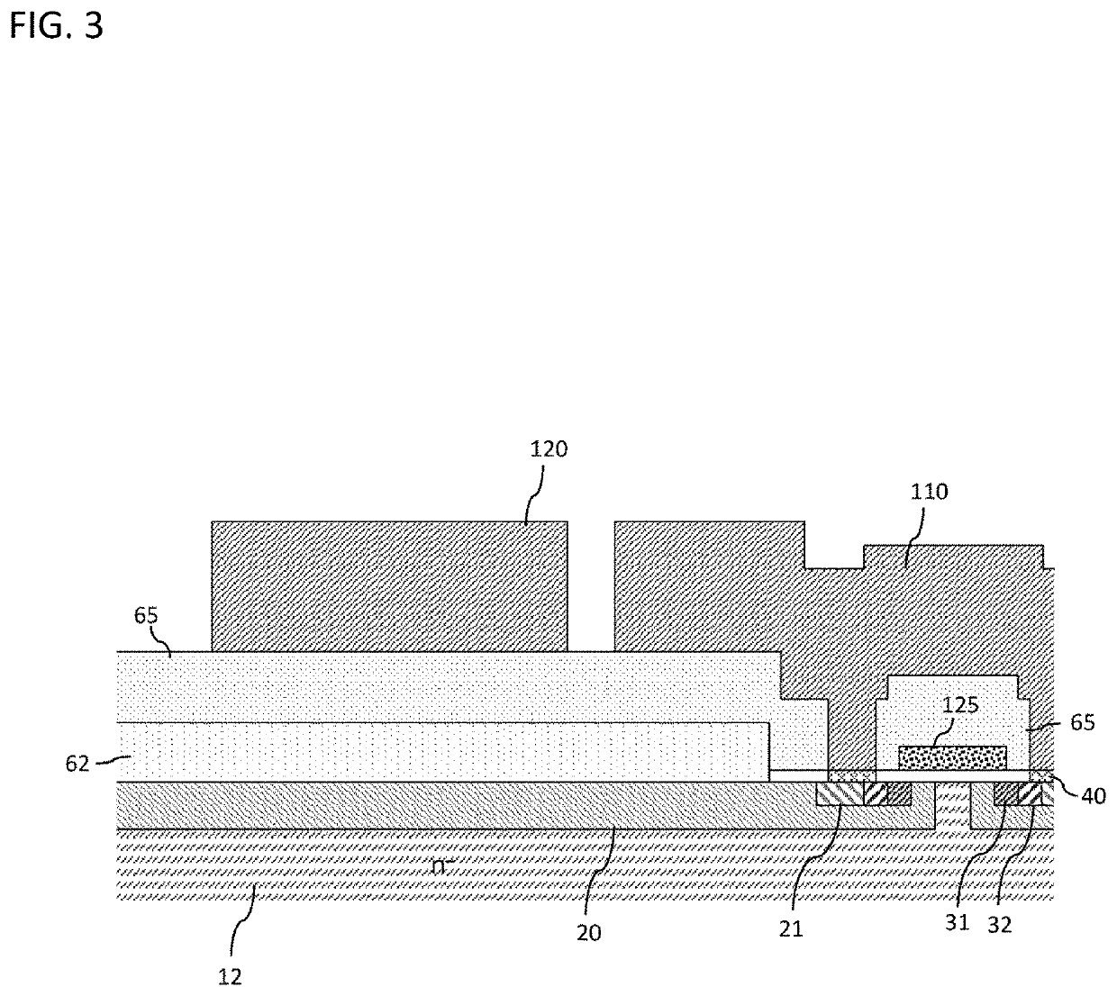
[0079]Next, a third embodiment of the present invention will be described.
[0080]In the present embodiment, as illustrated in FIG. 5, a polysilicon layer 150 has a lightly-doped polysilicon layer 153 in contact with a drift layer 12, and a heavily-doped polysilicon layer 154 that is provided on the lightly-doped polysilicon layer 153 and has an impurity concentration higher than an impurity concentration of the lightly-doped polysilicon layer 153. Various configurations employed in the above-described embodiments can be employed also in the present embodiment. The members described in the above embodiments will be described with the same reference signs. Additionally, the impurity concentration of the lightly-doped polysilicon layer 153 is 1×10¹⁵ to 5×1018 cm−3, for example, and the impurity concentration of the heavily-doped polysilicon layer 154 is 5×10¹⁸ to 1×1021 cm−3, for example.
[0081]Also the present embodiment can produce effects similar to those produced by the second embodi...
PUM
| Property | Measurement | Unit |
|---|---|---|
| conductivity | aaaaa | aaaaa |
| concentration | aaaaa | aaaaa |
| conductivity type | aaaaa | aaaaa |
Abstract
Description
Claims
Application Information