Determining Sums Using Logic Circuits

a logic circuit and sum technology, applied in logic circuits, logic circuits, logic circuits characterised by logic functions, etc., can solve the problem that functions consume a large amount of available programmable logic resources

Active Publication Date: 2021-04-01
SUPERFASTFPGA LTD
View PDF0 Cites 0 Cited by
  • Summary
  • Abstract
  • Description
  • Claims
  • Application Information

AI Technical Summary

Benefits of technology

[0017]According to a second aspect of the present invention there is provided a logic circuit configured to determine the sum of a plurality of multiple-bit inputs, the logic circuit being configured to: receive the plurality of multiple-bit inputs; split at least one of the received multiple-bit inputs into two or more multiple-bit binary strings; route each of the two or more multiple-bit binary strings to a different adder for adding wherein each adder comprises a plurality of single-bit stages having insufficient capacity to add all possible combinations of bits in a respective bit position of the plurality of multiple-bit inputs; add an intermediate addition output having a contribution from one of the at least two binary strings to (i) the other(s) of the at least two binary strings, or (ii) at least one other intermediate addition output having a contribution from the other(s) of the at least two binary strings, so as to form a second output; determine the sum of the plurality of multiple bit input numbers in dependence on the second output; and output the sum of the plurality of multiple bit numbers.
[0018]The logic circuit may be further configured to split a multiple-bit input into two or more binary strings such that each bit of the split multiple-bit input contributes to only one of the binary strings and all of the bits of multiple bit input are allocated to a binary string.
[0019]The sum of the two or more binary strings may be equal to the multiple-bit input from which they are split.

Problems solved by technology

Owing to the widespread use of additions functions in many DSP applications and mathematical operations, these functions often consume a large amount of the available programmable logic resources on a programmable logic circuit.

Method used


Image

  • Determining Sums Using Logic Circuits
  • Determining Sums Using Logic Circuits
  • Determining Sums Using Logic Circuits

Examples


Embodiment Construction

[0050]The following description is presented by way of example to enable a person skilled in the art to make and use the invention. The present invention is not limited to the embodiments described herein and various modifications to the disclosed embodiments will be apparent to those skilled in the art. Embodiments are described by way of example only.

[0051]The examples described herein are be described with reference to a field programmable gate array (FPGA) as an example of a programable logic device (PLD). It is to be understood that the principles described herein could be applied to any other type of logic device, or programmable logic device (PLD).

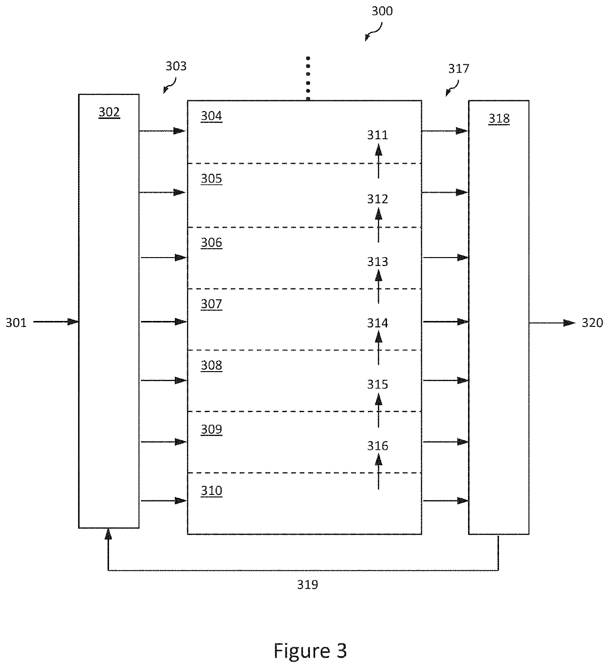
[0052]FIG. 3 is a simplified schematic of a field programmable gate array (FPGA) 300. In the example shown in FIG. 3, FPGA 300 comprises an input routing block 302, an output routing block 318, and a column of configurable logic blocks (CLBs) 304-310. Although shown separately, input routing block 302 and an output routing block 318...


PUM


Abstract

A logic circuit comprising: inputs for receiving multiple n-bit numbers, n being greater than one; and an adder capable of receiving m n-bit numbers, m being greater than one, and forming an output representing the sum of those numbers, the adder having a plurality of single-bit stages and being configured to form the sum by subjecting successive bits of each of the numbers to an operation in a respective one of the single-bit stages, the single-bit stages being such that the adder has insufficient capacity to add all possible combinations of bits in a respective bit position of m n-bit numbers; the addition circuit being configured to add the multiple n-bit numbers by: in the adder, adding a first one of the n-bit numbers to a value corresponding to a set of non-consecutive bits of another of the n-bit numbers to form a first intermediate value; adding the first intermediate value to a value corresponding to the bits of the said other of the n-bit numbers other than those in the said set to form a sum; and outputting the sum.

Description

CLAIM OF PRIORITY[0001]The present application claims priority to GB Patent Application Serial No. 1913979.9, filed on Sep. 27, 2019, the entire contents of which are hereby incorporated by reference.BACKGROUND[0002]The present invention relates to apparatus and methods for determining a sum of a plurality of multiple bit binary inputs using logic devices.[0003]Logic devices can be used to perform logic functions. Programmable logic devices (PLDs) are a type of integrated circuit that can be programmed to perform specified logic functions. A field programmable gate array (FPGA) is one type of PLD. An FPGA is a semiconductor device that comprises a matrix of configurable logic blocks (CLBs) connected via programmable interconnects. An FPGA can be programmed by providing configuration instructions which determine the function of the programmable elements of the FPGA. Configuration instructions may be in the form of configuration data loaded into an internal memory cell of the FPGA. On...

Claims


Application Information

Patent Timeline
Patent Type & Authority Applications(United States)
IPC IPC(8): H03K19/17704H03K19/20G06F7/501G06F1/03
CPCH03K19/17708G06F1/03G06F7/501H03K19/20G06F7/509G06F7/5057
Inventor METZGEN, PAUL JAMES
Owner SUPERFASTFPGA LTD
Why Eureka
Try Eureka