Probe card for high frequency applications

a high-frequency, probe-based technology, applied in the field of probe-based cards, can solve the problems of the probe itself, the length of the probe body, and the stiffness of the probe, and achieve the effect of removing the risk of breaking, deformation and/or movemen

Active Publication Date: 2021-04-29
TECHNOPROBE
View PDF0 Cites 5 Cited by
  • Summary
  • Abstract
  • Description
  • Claims
  • Application Information

AI Technical Summary

Benefits of technology

[0042]The probe card is configured to carry high frequency signals without adding any noise to these signals, meanwhile ensuring a correct working thereof during the contact of the relevant contact probes with the pads of a device under test, removing the risk of breaking, deformation and / or movement of the membrane which these contact probes are associated with, in particular at a peripheral portion thereof providing a mechanical and electrical contact, so overcoming the problems tied to the prior art solutions.

Problems solved by technology

This problem is particularly felt in the case of the so-called short probes, i.e., probes with a limited-length body, in particular with a size of less than 5000 μm.
However, the reduced length of the body of the probes dramatically increases the stiffness of the probe itself, which involves an increase of the force exerted by the respective contact tip on the contact pads of a device under test, which can lead to a breaking of these pads, with irreparable damage of the device under test, a situation to be obviously avoided.
Even more dangerously, the increase in the stiffness of the contact probe due to the reduction of the length of the body thereof also increases the risk of breaking the probes themselves.
It is nevertheless well known that these contacts made by welds, conductive glues or rubbers, screws actually cause of serious troubles when carrying high frequency signals, such as radiofrequency signals, actually providing probe cards as a whole not very performing.
These known solutions, providing a fixed association between the membrane and the support plate or testing apparatus, have subsequent problems linked to the movement and to the deformation of the membrane itself during the testing operations when the probe card is in pressing contact with the semiconductor wafer.
These stresses existing at the peripheral portion 22C of the membrane 22 increase the risks of breaking it, possibly local micro-breakings.

Method used


Image

  • Probe card for high frequency applications
  • Probe card for high frequency applications
  • Probe card for high frequency applications

Examples


Embodiment Construction

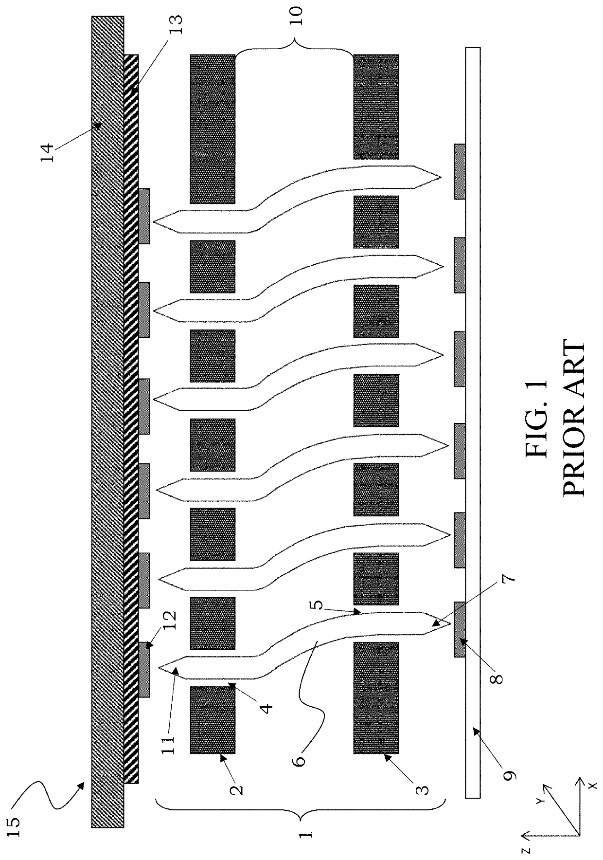
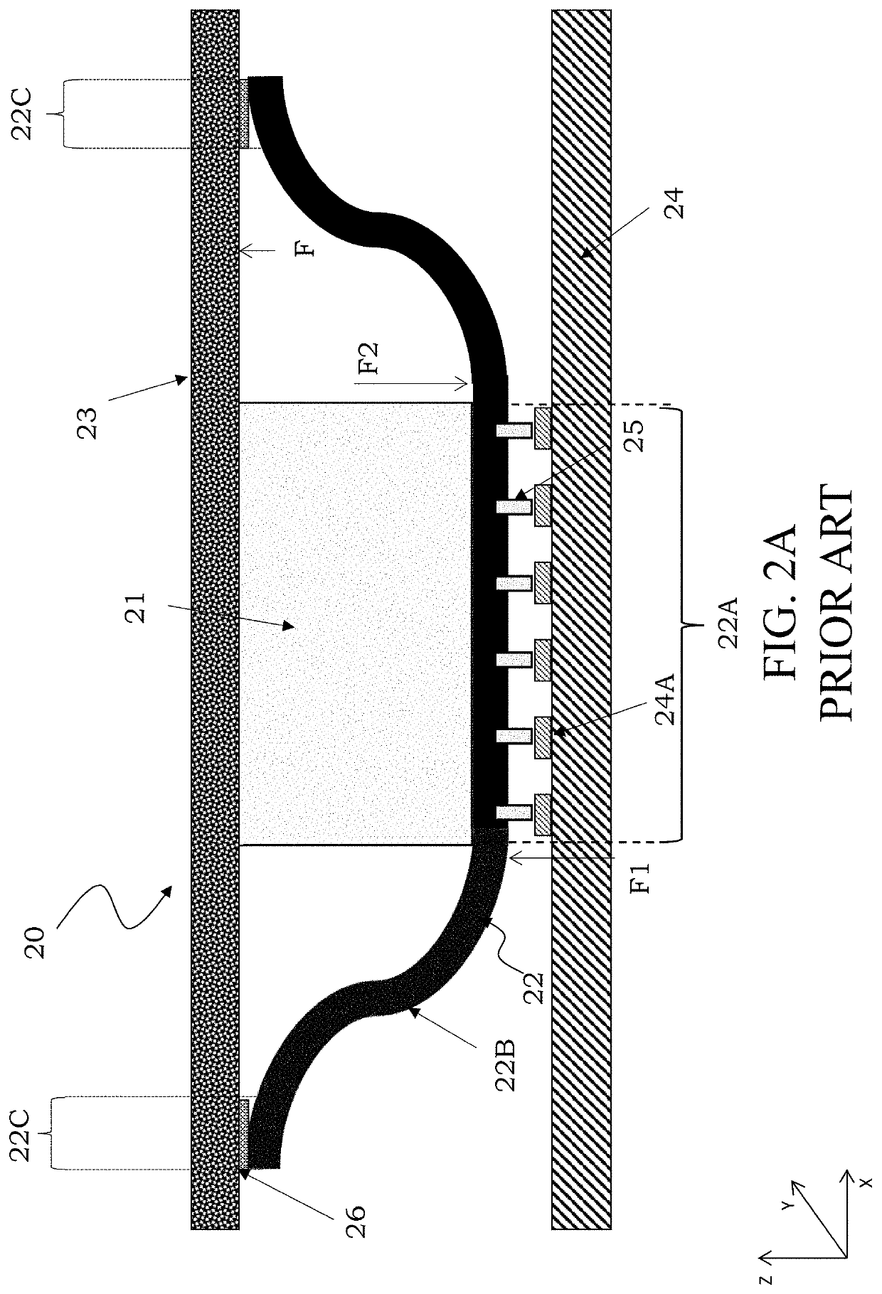
[0075]With reference to the figures, and particularly to FIGS. 3A and 3B, a probe card realized according to the present disclosure is globally and schematically indicated with 30.

[0076]It should be noted that the figures are schematic views and are not drawn to scale, but they are instead drawn so as to emphasize the important features of the disclosure. Furthermore, in the figures, the different elements are schematically depicted, the shape thereof being changeable depending on the desired application. Moreover, it should be noted that in the figures identical reference numbers refer to identical elements in terms of shape or function. Finally, special arrangements described in relation to an embodiment shown in a figure can also be used for the other embodiments shown in the other figures.

[0077]In its most general form, the probe card 30 is configured to connect to an equipment (not shown in the figures) to perform the test of electronic devices integrated on a semiconductor waf...


PUM


Abstract

A probe card for testing a device under test having a plurality of contact pads includes a support plate having first contact pads thereon. A flexible membrane has a first face and a peripheral portion including second contact pads thereon. A plurality of contact probes are associated with a first face of the flexible membrane and are configured to abut onto the plurality of contact pads of the device under test. A sliding contact area includes: the first contact pads formed on the support plate; the second contact pads formed on the peripheral portion of the flexible membrane, the peripheral portion of the flexible membrane configured to come in pressing contact onto the support plate at the sliding contact area. A pressing element contacts the peripheral portion of the flexible membrane at the sliding contact area, and the pressing element puts the second contact pads into pressing contact with the first contact pads.

Description

BACKGROUNDTechnical Field[0001]The present disclosure relates to a probe card for testing electronic devices integrated on a semiconductor wafer.[0002]More particularly, the present disclosure relates to a probe card comprising at least one support plate for the connection to the testing apparatus as well as a flexible membrane and a plurality of contact probes associated with a first face thereof, these contact probes being configured to abut onto a plurality of contact pads of a device under test integrated on a semiconductor wafer and being configured to carry high frequency signals.[0003]The following description is made with reference to this field of application with the only purpose of simplifying the exposition thereof.Description of the Related Art[0004]As it is well known, a probe card is essentially a device configured to electrically connect a plurality of contact pads of a microstructure, in particular an electronic device integrated on a semiconductor wafer, with corre...

Claims


Application Information

Patent Timeline
Patent Type & Authority Applications(United States)
IPC IPC(8): G01R1/073G01R1/067
CPCG01R1/0735G01R1/06772G01R1/07314G01R1/07357
Inventor VETTORI, RICCARDO
Owner TECHNOPROBE
Why Eureka
Try Eureka