Data processing system and operation method of data processing system

Active Publication Date: 2021-04-29
SEMICON ENERGY LAB CO LTD
View PDF0 Cites 0 Cited by
  • Summary
  • Abstract
  • Description
  • Claims
  • Application Information

AI Technical Summary

Benefits of technology

The patent text aims to provide a data processing system that can handle a large amount of data and has a high-speed operation while reducing the size, power consumption, and cost of the system. One of the technical effects of the patent is to provide a system with a main memory device that has a small storage capacity but can be increased when the system is activated. This allows for a flexible and cost-effective data processing system that can handle large data sets.

Problems solved by technology

Therefore, when the OS transistor is used in the memory cell of DRAM, stored data can be held for a long time.

Method used


Image

  • Data processing system and operation method of data processing system
  • Data processing system and operation method of data processing system
  • Data processing system and operation method of data processing system

Examples


embodiment 1

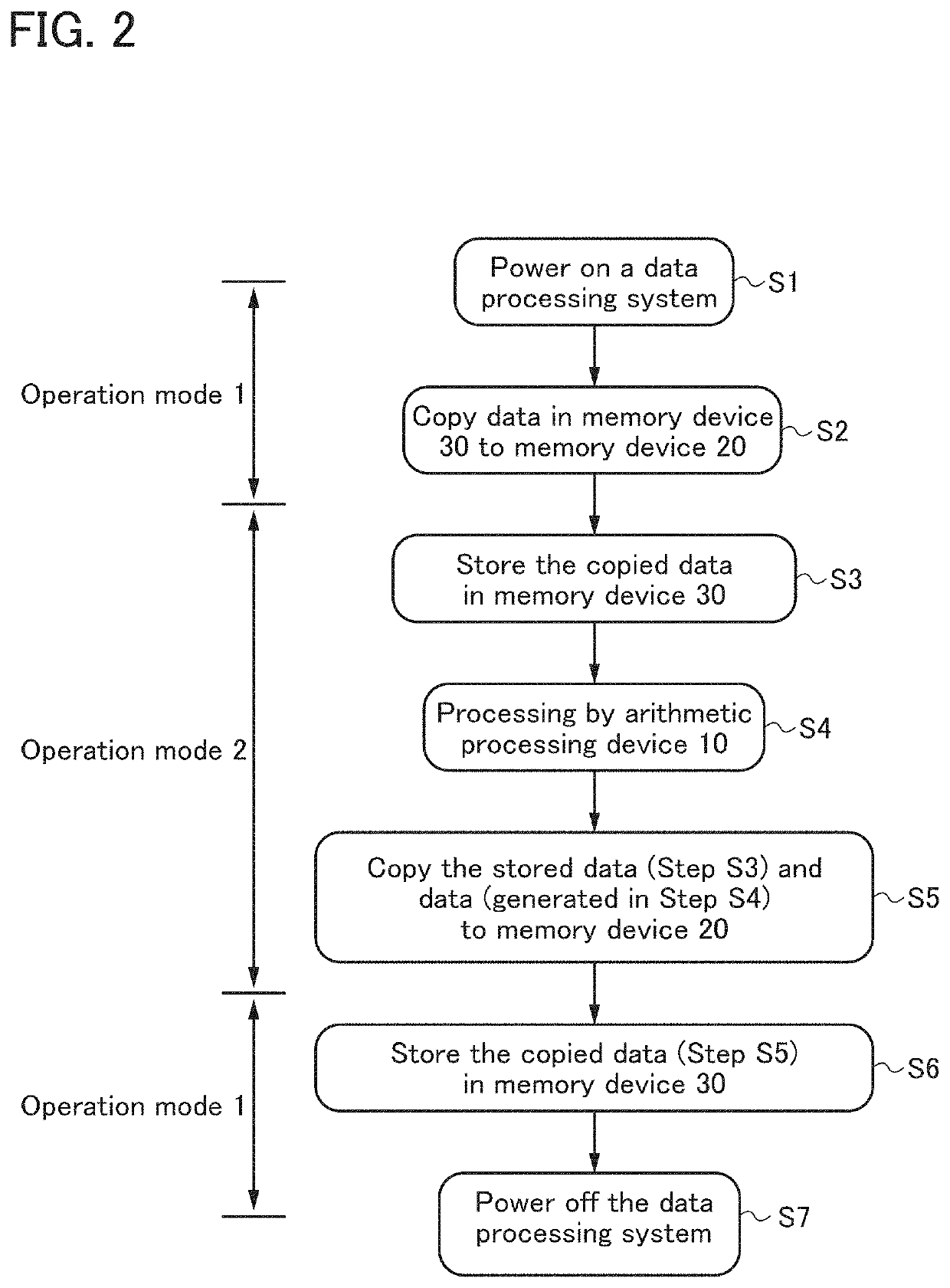
[0070]In this embodiment, a structure example and an operation example of data processing system which is one embodiment of the present invention will be described.

Structure Example of Data Processing System

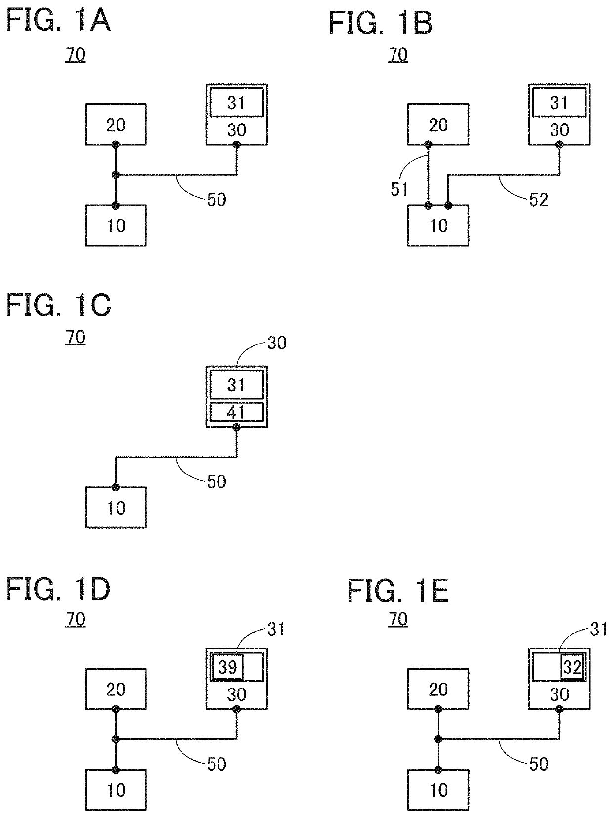
[0071]FIG. 1A is a block diagram illustrating a structure example of a data processing system 70 of one embodiment of the present invention. The data processing system 70 includes an arithmetic processing device 10, a memory device 20, and a memory device 30.

[0072]The arithmetic processing device 10, the memory device 20, and the memory device 30 are connected with a bus 50, and data can be transmitted therebetween. The memory device 20 and the memory device 30 may be connected to each other via the arithmetic processing device 10. Specifically, in the data processing system 70 as illustrated in FIG. 1B, the arithmetic processing device 10 and the memory device 20 may be connected with a bus 51, and the arithmetic processing device 10 and the memory device 30 may be connected wit...

embodiment 2

[0090]In Embodiment 2 and Embodiment 3, a structure example and an operation example of a memory device 270 according to one embodiment of the present invention will be described. The memory device 270 is an example of a memory device that can be used for the above-described memory device 30 and includes a gain-cell memory cell using an OS transistor. In other words, the memory device 270 is an NOSRAM as described above.

[0091]Note that a memory device that can be used for the memory device 30 is not limited to the memory device 270. For example, a memory device including a memory cell composed of one OS transistor and one capacitor or a memory device such as a NAND flash memory, a NOR flash memory, a magnetoresistive RAM (MRAM), a phase change RAM (PRAM), a resistive RAM (ReRAM), or a ferroelectric RAM (FeRAM) may be used. Alternatively, a combination of any of the memory devices may be used.

[0092]In Embodiment 2, examples of circuit structures and operations of a memory cell includ...

example 2

Memory Cell Structure Example 2

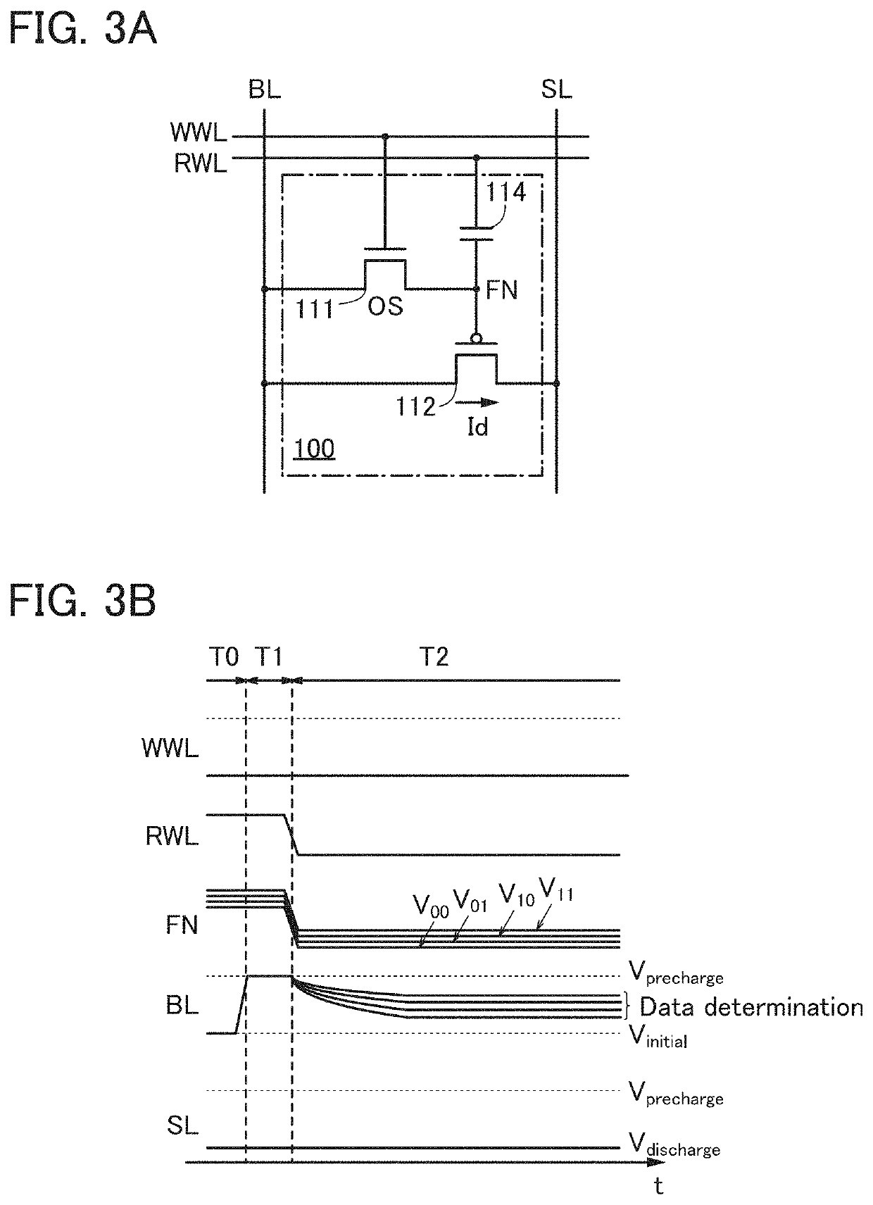
[0126]The memory cell 100 may include the transistor 111, the capacitor 114, and an n-channel transistor 113. FIG. 4A illustrates a structure example in which the memory cell 100 includes the transistor 111, the capacitor 114, and the transistor 113.

[0127]A gate of the transistor 111 is connected to a write word line WWL. One of a source and a drain of the transistor 111 is connected to a bit line BL. The other of the source and the drain of the transistor 111 is connected to a floating node FN.

[0128]A gate of the transistor 113 is connected to the floating node FN. One of a source and a drain of the transistor 113 is connected to a read word line RWL. The other of the source and the drain of the transistor 113 is connected to a bit line RBL.

[0129]One electrode of the capacitor 114 is connected to the floating node FN. The other electrode of the capacitor 114 is connected to a wiring CAL to which a predetermined potential is supplied.

[0130]When the mem...


PUM


Abstract

To provide a data processing system that includes a nonvolatile memory device capable of storing multilevel data and enables increasing storage capacity of a main memory device when the data processing system is activated. The data processing system includes an arithmetic processing device, a main memory device, and a nonvolatile memory device. The main memory device includes a volatile memory device, and the nonvolatile memory device is configured to store multilevel data in one memory cell. When the data processing system is deactivated, the nonvolatile memory device stores binary data, whereby the stored data can be held for a long time. Upon activation, the nonvolatile memory device stores multilevel data, whereby increasing storage capacity. When the storage capacity is increased, a free space is generated in the nonvolatile memory device, which can be used as a part of the main memory device of the data processing system.

Description

BACKGROUND OF THE INVENTION1. Field of the Invention[0001]The present invention relates to a data processing system. In particular, the present invention relates to a data processing system including a memory device (also referred to as a semiconductor memory device or memory) utilizing semiconductor characteristics.[0002]Note that one embodiment of the present invention is not limited to the above technical field. The technical field of the invention disclosed in this specification and the like relates to an object, a method, or a manufacturing method. Furthermore, one embodiment of the present invention relates to a process, a machine, manufacture, or a composition of matter.2. Description of the Related Art[0003]The data processing systems such as personal computers and portable information terminals such as smartphones, which have been used widely in recent years, for example, include arithmetic processing devices such as central processing units (CPUs) and graphics processing u...

Claims


Application Information

Patent Timeline
IPC IPC(8): G06F9/30G11C11/4093G11C11/402G11C11/408G11C11/4094
CPCG06F9/3001G06F9/3004G11C11/4094G11C11/4023G11C11/4085G11C11/4093G11C11/405G11C2211/5641G11C11/565
Inventor YAMAZAKI, SHUNPEIKIMURA, HAJIMEONUKI, TATSUYA
Owner SEMICON ENERGY LAB CO LTD
Why Eureka
Try Eureka