Method for producing organic electroluminescent display device comprising polydiacetylene layers

a polydiacetylene and display device technology, applied in the direction of organic semiconductor devices, identification means, instruments, etc., can solve the problems of limited bendability and uneven display of the display device, and achieve the effect of improving the color purity of the blue pixel and the red pixel

Active Publication Date: 2021-05-13
SAKAI DISPLAY PROD
View PDF0 Cites 2 Cited by
  • Summary
  • Abstract
  • Description
  • Claims
  • Application Information

AI Technical Summary

Benefits of technology

[0030]An embodiment of the present invention provides an organic EL display device having an

Problems solved by technology

An OLED (especially, an organic light emitting layer and a cathode electrode material) is easily influenced by moisture to be deteriorated and to

Method used


Image

  • Method for producing organic electroluminescent display device comprising polydiacetylene layers
  • Method for producing organic electroluminescent display device comprising polydiacetylene layers
  • Method for producing organic electroluminescent display device comprising polydiacetylene layers

Examples


Embodiment Construction

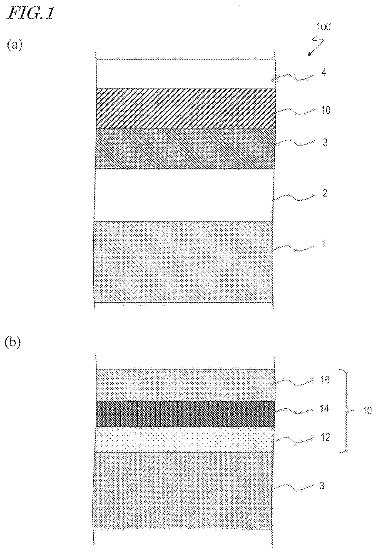
[0037]Hereinafter, an OLED display device and a method for producing the same according to embodiments of the present invention will be described with reference to the drawings. The embodiments of the present invention are not limited to the embodiments that are described below as examples. For example, an organic EL display device according to an embodiment of the present invention may include, for example, a glass substrate instead of a flexible substrate.

[0038]First, with reference to FIG. 1(a) and FIG. 1(b), a basic structure of an OLED display device 100 according to an embodiment of the present invention will be described. FIG. 1(a) is a schematic partial cross-sectional view of an active region of the OLED display device 100 according to an embodiment of the present invention. FIG. 1(b) is a partial cross-sectional view of a TFE structure 10 formed on an OLED 3.

[0039]The OLED display device 100 includes a plurality of pixels, and each of the pixels includes at least one organ...


PUM

PropertyMeasurementUnit
Thicknessaaaaaaaaaa
Thicknessaaaaaaaaaa
Nanoscale particle sizeaaaaaaaaaa

Abstract

This organic EL display device (100) is provided with an element substrate which comprises multiple pixels and which comprises organic EL elements (3) arranged in each pixel and bank layers (48) defining the pixels, and a thin-film sealing structure (10) which covers the pixels. The thin-film sealing structure includes a first inorganic barrier layer (12), and an organic barrier layer (14) in contact with the upper surface or lower surface of the first inorganic barrier layer. The multiple pixels include red pixels, green pixels and blue pixels, and further have a first polydiacetylene layer (52a) which exhibits a blue color and which is provided selectively on a second inorganic barrier layer (16) of the thin-film sealing structure on blue pixels, and a second polydiacetylene layer (52b) which exhibits a red color and which is provided selectively on the thin-film sealing structure on red pixels. The first and second polydiacetylene layers are a polymer of 10,12-pentacosadiynoic acid.

Description

TECHNICAL FIELD[0001]The present invention relates to an organic EL display device and a method for producing the same.BACKGROUND ART[0002]Organic EL (Electroluminescence) display devices start being put into practical use. One feature of an organic EL display device is flexibility thereof. Such an organic EL display device includes, in each of pixels, at least one organic EL element (Organic Light Emitting Diode: OLED) and at least one TFT (Thin Film Transistor) controlling an electric current to be supplied to the at least one OLED. Hereinafter, an organic EL display device will be referred to as an “OLED display device”. Such an OLED display device including a switching element such as a TFT or the like in each of OLEDs is called an “active matrix OLED display device”. A substrate including the TFTs and the OLEDs will be referred to as an “element substrate”.[0003]An OLED (especially, an organic light emitting layer and a cathode electrode material) is easily influenced by moistu...

Claims


Application Information

Patent Timeline
IPC IPC(8): H01L27/32H01L51/52H01L51/56H01L51/00
CPCH01L27/322H01L51/5253H01L2251/558H01L51/0041H01L51/56G09F9/00G09F9/30H05B33/04H05B33/10H05B33/12H10K59/38H10K50/8445H10K50/86H10K50/844H10K71/00H10K85/143H10K2102/351
Inventor KISHIMOTO, KATSUHIKOKATO, TAKUJI
Owner SAKAI DISPLAY PROD
Why Eureka
Try Eureka