
Crosslinkable polymeric materials for dielectric layers in electronic devices

a technology of electronic devices and polymeric materials, applied in semiconductor devices, solid-state devices, capacitors, etc., can solve the problems of inability to cure dielectric layers in ofet devices, inability to apply incompatible solvents, and inability to meet the requirements of uv-cured dielectric layers

Inactive Publication Date: 2021-05-13
ALTANA
View PDF4 Cites 0 Cited by
  • Summary
  • Abstract
  • Description
  • Claims
  • Application Information

AI Technical Summary

Benefits of technology

The use of aliphatic polymers with DCPD functionalities results in stable, effectively crosslinked dielectric layers that enhance the performance and compatibility of OFETs by improving adhesion and reducing dipolar interactions, leading to improved device performance and stability under UV exposure.

Problems solved by technology

Polyimides do indeed have excellent dielectric properties, but their limited solubility means that they can often only be applied from incompatible solvents such as N-methyl-2-pyrrolidone (NMP).
Polycycloolefins, such as polynorbornenes, for example, do have excellent dielectric properties, but the adhesion is often limited on account of their high glass transition temperature, especially on non-polar organic semiconductor films.
These compositions are not suited for use as UV-cured dielectric layers in OFET devices.
The resin compositions are not suited for use as dielectric layers in OFET devices.

Method used


Image

  • Crosslinkable polymeric materials for dielectric layers in electronic devices
  • Crosslinkable polymeric materials for dielectric layers in electronic devices
  • Crosslinkable polymeric materials for dielectric layers in electronic devices

Examples


example a1 preparation

of Polymer 1

[0113]Using a syringe technique, 20 ml of freshly distilled dicyclopentenyloxyethyl methacrylate (FA-512M, Hitachi Chemical) and 20 ml of THF were transferred under argon into a two-necked flask. Then 30 mg of 2,2′-azobisisobutyronitrile in the form of a THF solution were added, and the mixture was heated to 60° C. with stirring. After six hours, the reaction was discontinued by addition of 50 mg of butylated hydroxytoluene (BHT) and cooling to room temperature. The polymerization solution was precipitated from 1000 ml of methanol, and the polymer was isolated by filtration and dried under reduced pressure. The polymer was then dissolved again three times in 100 ml of THF and precipitated from 800 ml of methanol with addition of 20 mg of BHT each time.

[0114]Yield 20.2%

[0115]Mn=219 000 g / mol, Mw=520 000 g / mol

[0116]Tg=61° C.

example a2 preparation

of Polymer 2

[0117]Using a syringe technique, 20 ml of freshly distilled dicyclopentenyl methacrylate (CD535, Sartomer) and 20 ml of THF were transferred under argon into a two-necked flask. Then 40 mg of 2,2′-azobisisobutyronitrile in the form of a THF solution were added, and the mixture was heated to 50° C. with stirring. After ten hours, the reaction was discontinued by addition of 50 mg of butylated hydroxytoluene (BHT) and cooling to room temperature. The polymerization solution was precipitated from 1000 ml of methanol, and the polymer was isolated by filtration and dried under reduced pressure. The polymer was then dissolved again three times in 100 ml of THF and precipitated from 800 ml of methanol with addition of 20 mg of BHT each time.

[0118]Yield 18.5%

[0119]Mn=89 600 g / mol, Mw=237 000 g / mol

[0120]Tg=178° C.

example a3 preparation

of Polymer 3

[0121]Using a syringe technique, 10 ml of freshly distilled dicyclopentenyloxyethyl methacrylate (FA-512M, Hitachi Chemical), 10 ml of freshly distilled methyl methacrylate and 40 ml of THF were transferred under argon into a two-necked flask. Then 30 mg of 2,2′-azobisisobutyronitrile in the form of a THF solution were added, and the mixture was heated to 50° C. with stirring. After eight hours, the reaction was discontinued by addition of 50 mg of BHT and cooling to room temperature. The polymerization solution was precipitated from 1000 ml of methanol, and the polymer was isolated by filtration and dried under reduced pressure. The polymer was then dissolved again three times in 100 ml of THF and precipitated from 800 ml of methanol with addition of 20 mg of BHT each time.

[0122]Yield 35%

[0123]Mn=87 700 g / mol, Mw=317 000 g / mol

[0124]Tg=94° C.

[0125]Repeating units in the polymer: FA-512M / MMA ratio 28:72 (determined via 1H-NMR)


PUM

PropertyMeasurementUnit
mol %aaaaaaaaaa
temperatureaaaaaaaaaa
atmospheric pressureaaaaaaaaaa

Abstract

Compositions for providing a dielectric layer in an electronic device wherein the composition comprises a polymer which polymer contains one or more building blocks, wherein at least 25 mol % of the total number of building blocks in the polymer are of the general formula having olefinic oligo-dihydrodicyclopentadienyl functionalities.

Description

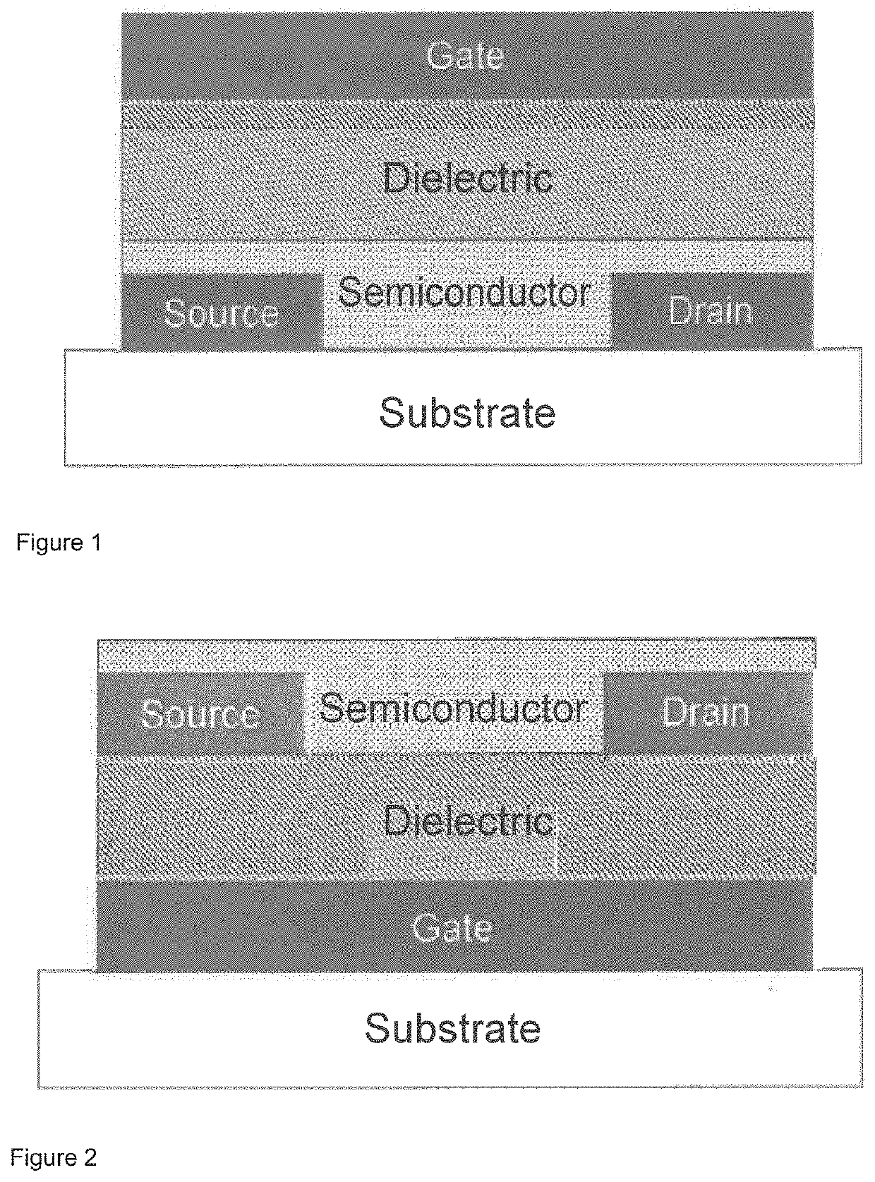
[0001]All of the documents cited in the present patent application are incorporated by reference in their entirety into the present disclosure.[0002]The present invention relates to crosslinkable polymers, dielectric layers comprising them, electronic devices, more particularly organic field-effect transistors, comprising them.PRIOR ART[0003]Organic field-effect transistors (OFETs) are electronic devices which find application in flexible displays, sensor devices or electronic circuits.[0004]An OFET is a multilayer device which comprises a substrate, a source electrode and drain electrode, an organic semiconductor layer, a dielectric layer and a gate electrode. The semiconductor layer typically comprises an organic polymer and / or a small molecule.[0005]Depending on the arrangement of the layers in an OFET, a distinction is made between a top gate and a bottom gate configuration. In the top gate configuration, the semiconductor layer is followed by the dielectric and lastly by the ga...

Claims


Application Information

Patent Timeline
Patent Type & Authority Applications(United States)
IPC IPC(8): H01L51/05C08F12/18C08F12/32C08F20/22C08F20/28C08F20/40H01L51/00H10N97/00
CPCH01L51/052C08F12/18C08F12/32C08F20/22H01L28/40C08F20/40H01L51/004H01L51/0043C08F20/28H10K10/471H10K85/151H10K85/141
Inventor EGGERT, MARTINFESER, STEPHANTÖDTER-KÖNIG, SASCHA
Owner ALTANA
Learn More