
Light emitting element, display device including the same, and method for manufacturing the display device

a technology of light emitting elements and display devices, applied in the direction of organic chemistry, group 3/13 element organic compounds, nanostructure assemblies, etc., can solve the problems of low blue light efficiency and easy exposure of organic materials to high-temperature operating environments, and achieve the effect of improving the alignment of light emitting elements and increasing dielectrophoretic reactivity

Pending Publication Date: 2021-07-01
SAMSUNG DISPLAY CO LTD
View PDF0 Cites 10 Cited by
  • Summary
  • Abstract
  • Description
  • Claims
  • Application Information

AI Technical Summary

Benefits of technology

The patent text explains a light emitting element that has a higher dielectric anisotropy, which improves the alignment of the light emitting elements when manufacturing a display device. This is achieved by bonding an element orienter that can form an intra-molecular dipole to the light emitting element. The higher dielectric anisotropy, in turn, increases the reactivity of the light emitting element when aligned between electrodes, making the manufacturing process more efficient.

Problems solved by technology

However, it is known that the organic material is vulnerable to a high-temperature operating environment and the blue light efficiency is relatively low.
Also, in the manufacturing process, as noted as a drawback of a conventional inorganic light emitting diode, a transfer method using a dielectrophoresis (DEP) method has been developed.

Method used


Image

  • Light emitting element, display device including the same, and method for manufacturing the display device
  • Light emitting element, display device including the same, and method for manufacturing the display device
  • Light emitting element, display device including the same, and method for manufacturing the display device

Examples


Embodiment Construction

[0046]Embodiments of the present disclosure will now be described more fully hereinafter with reference to the accompanying drawings, in which embodiments of the present disclosure are shown. The subject matter of the present disclosure may, however, be embodied in different forms and should not be construed as limited to the embodiments set forth herein. Rather, these embodiments are provided so that this disclosure will be thorough and complete, and will fully convey the scope of the present disclosure to those skilled in the art.

[0047]It will also be understood that when a layer is referred to as being “on” another layer or substrate, it can be directly on the other layer or substrate, or intervening layers may also be present. The same reference numbers indicate the same components throughout the specification.

[0048]It will be understood that, although the terms “first,”“second,” etc. may be used herein to describe various elements, these elements should not be limited by these ...


PUM


Abstract

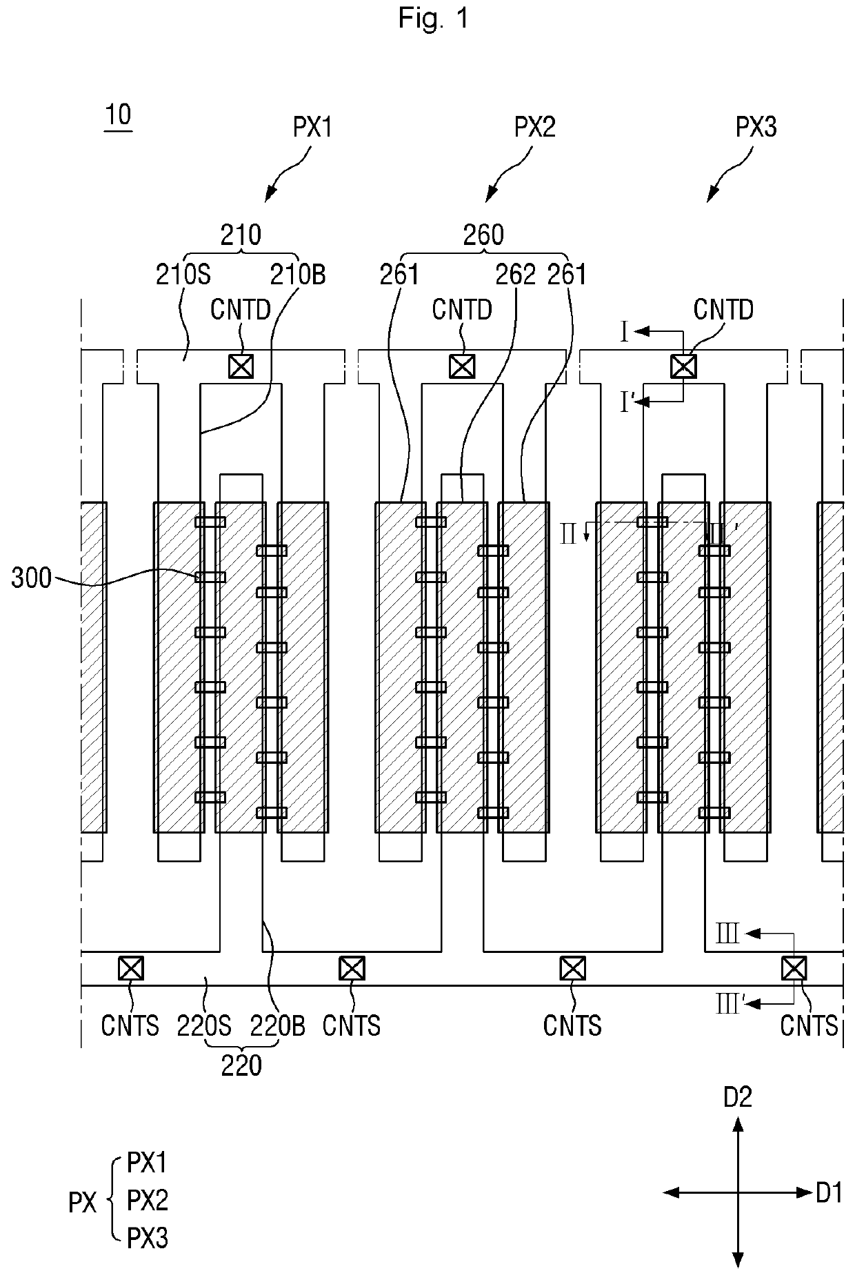
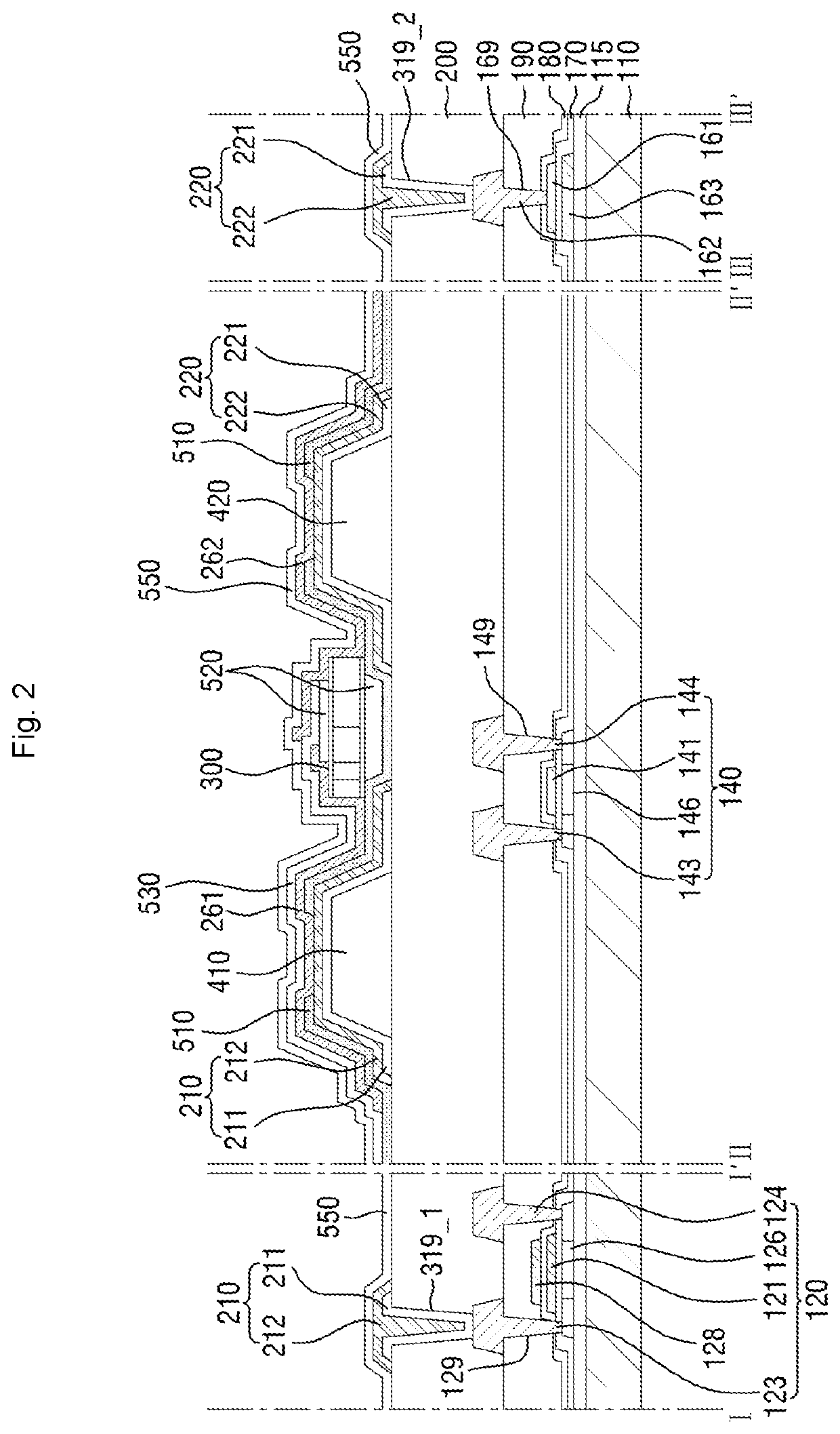
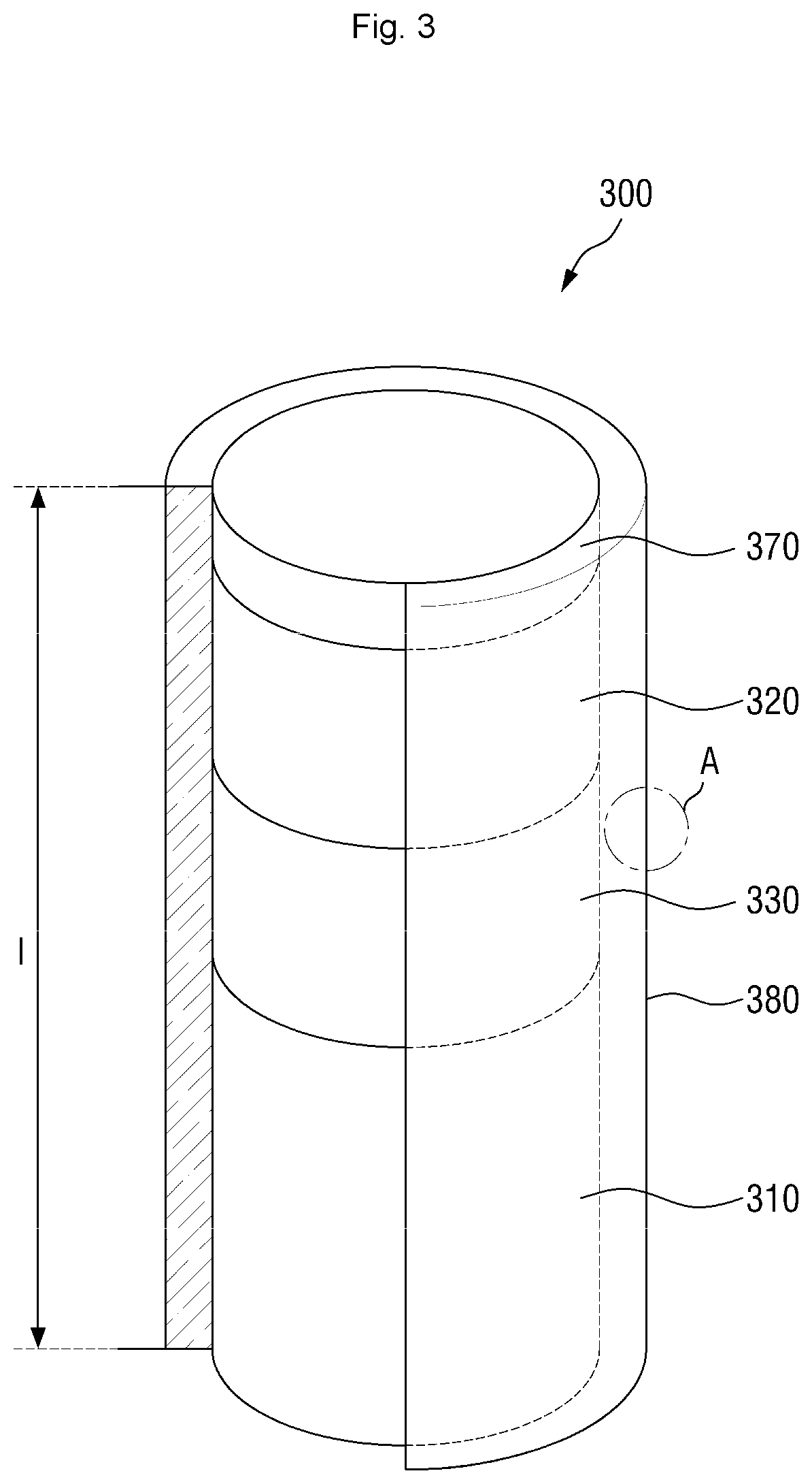
A light emitting device, a display device comprising same, and a method for manufacturing a display device are provided. The light emitting device comprises: a first conductivity type semiconductor doped to have a first polarity, an active layer on the first conductivity type semiconductor, a second conductivity type semiconductor on the active layer and doped to have a second polarity different from the first polarity and an insulating material layer surrounding side surfaces of the first conductivity type semiconductor, the second conductivity type semiconductor, and the active layer, wherein the insulating material layer includes an insulating material film and an element orienter bonded to an outer peripheral surface of the insulating material film.

Description

CROSS-REFERENCE TO RELATED APPLICATION[0001]This application is a U.S. National Phase Patent Application of Korean International Application No. PCT / KR2019 / 000115, filed Jan. 3, 2019, which claims priority to Korean Patent Application No. 10-2018-0099339, filed on Aug. 24, 2018, in the Korean Intellectual Property Office, the entire content of all of which is hereby incorporated by reference.TECHNICAL FIELD[0002]Embodiments of the present disclosure relate to a light emitting element, a display device including the same, and a method for manufacturing the display device, and more particularly, to a light emitting element having an increased dielectric anisotropy by an element orienter bonded to an outer surface thereof, a display device including the same and a method for manufacturing the display device.BACKGROUND[0003]The importance of display devices has steadily increased with the development of multimedia technology. Accordingly, various types of display devices such as an orga...

Claims


Application Information

Patent Timeline
IPC IPC(8): H01L33/44H01L25/075H01L27/12H01L33/24H01L33/38H01L33/62B82B3/00C07F7/18C07F5/02
CPCH01L33/44H01L25/0753H01L27/1214H01L33/24H01L33/38H01L2933/0066B82B3/0052C07F7/1804C07F5/027H01L2933/0016H01L2933/0025H01L33/62C07F5/025H10K85/658H01L33/56H01L33/02H01L27/156H10K85/40
Inventor JUNG, JAE HOONJO, SUNG CHAN
Owner SAMSUNG DISPLAY CO LTD
Learn More